
5AGXBA7D4F35C4G
| Part Description |
Arria V GX Field Programmable Gate Array (FPGA) IC 544 15470592 242000 1152-BBGA, FCBGA |
|---|---|
| Quantity | 196 Available (as of June 18, 2026) |
| Product Category | Field Programmable Gate Array (FPGA) |
|---|---|
| Manufacturer | Intel |
| Manufacturing Status | Active |
| Manufacturer Standard Lead Time | 12 Weeks |
| Datasheet |
Specifications & Environmental
| Device Package | 1152-FBGA, FC (35x35) | Grade | Commercial | Operating Temperature | 0°C – 85°C | ||
|---|---|---|---|---|---|---|---|
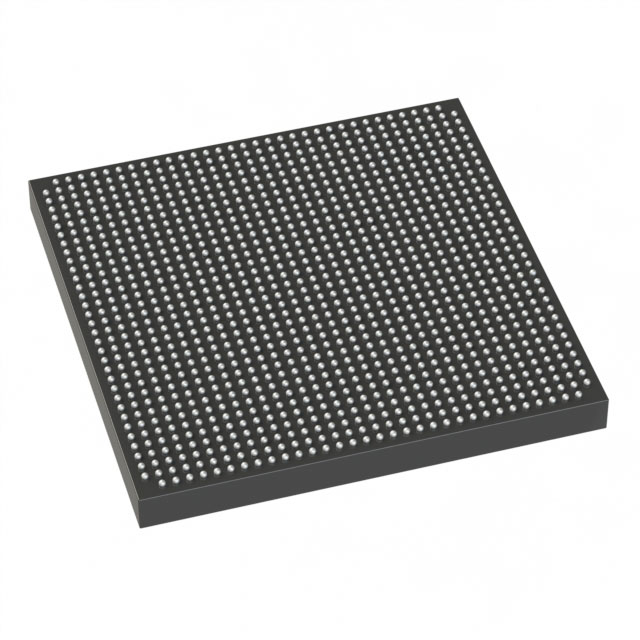
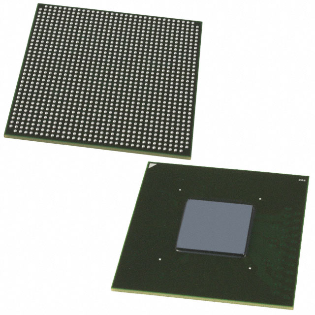
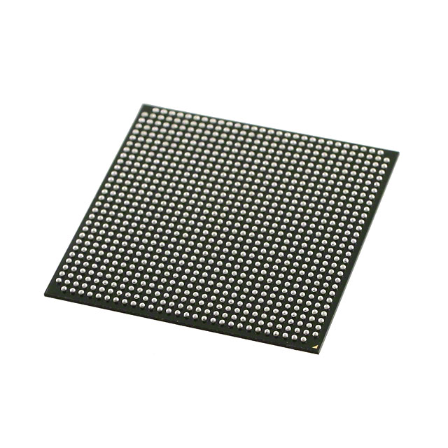
| Package / Case | 1152-BBGA, FCBGA | Number of I/O | 544 | Voltage | 1.07 V - 1.13 V | ||
| Mounting Method | Surface Mount | RoHS Compliance | RoHS Compliant | REACH Compliance | REACH Unaffected | ||
| Moisture Sensitivity Level | 3 (168 Hours) | Number of LABs/CLBs | 11460 | Number of Logic Elements/Cells | 242000 | ||
| Number of Gates | N/A | ECCN | PENDING ECCN | HTS Code | 0000.00.0000 | ||
| Qualification | N/A | Total RAM Bits | 15470592 |
Overview of 5AGXBA7D4F35C4G – Arria V GX Field Programmable Gate Array (FPGA), 242,000 logic elements, 15,470,592 RAM bits, 544 I/Os
The 5AGXBA7D4F35C4G is an Intel Arria V GX Field Programmable Gate Array (FPGA) IC designed for high-capacity programmable logic implementations. It combines a large logic fabric, substantial on-chip RAM, and a high I/O count in a single surface-mount FCBGA package.
This commercial-grade device targets designs that require significant logic resources and memory bandwidth while maintaining a compact 1152-FBGA (35×35) footprint and defined operating and supply conditions.
Key Features
- Logic Capacity Offers 242,000 logic elements to implement complex programmable logic and custom hardware functions.
- Logic Array Size Equivalent to 11,460 LABs/CLBs for architectural planning and resource estimation.
- On-chip Memory Provides 15,470,592 total RAM bits to support buffering, LUT-based storage, and embedded memory structures.
- I/O Density 544 I/O pins to accommodate extensive peripheral interfacing and multiple parallel I/O channels.
- Power and Supply Specified core supply voltage range of 1.07 V to 1.13 V for predictable power design and board-level planning.
- Package & Mounting 1152-BBGA, FCBGA (supplier package: 1152-FBGA, FC 35×35) in a surface-mount form factor for compact system integration.
- Operating Conditions Commercial-grade device with an operating temperature range of 0 °C to 85 °C.
- Regulatory RoHS compliant.
Typical Applications
- High-density logic implementations Deploy the 242,000 logic elements to realize complex state machines, datapath logic, and custom accelerators within a single FPGA.
- Memory-heavy designs Leverage 15,470,592 RAM bits for buffering, large LUT-based storage, or on-chip data staging in streaming or packet-processing applications.
- Boards requiring abundant I/O Use 544 I/Os to connect multiple peripherals, parallel interfaces, or broad bus structures without external I/O expanders.
Unique Advantages
- Substantial programmable capacity: 242,000 logic elements enable integration of large, multi-function hardware designs into a single device, reducing component count.
- Large on-chip RAM: 15,470,592 RAM bits provide the memory resources needed for buffering and data path optimization without relying solely on external memory.
- High I/O count: 544 I/Os simplify board-level routing for complex systems and reduce the need for additional interface chips.
- Compact FCBGA footprint: The 1152-FBGA (35×35) package offers a high-density mounting option for space-constrained PCBs while retaining ample resources.
- Predictable power window: Narrow core supply range (1.07 V–1.13 V) helps streamline power-supply design and validation.
- RoHS compliant: Meets common lead-free assembly requirements for commercial electronic products.
Why Choose 5AGXBA7D4F35C4G?
This Intel Arria V GX FPGA balances large programmable logic capacity, significant on-chip memory, and a high I/O count in a single commercial-grade FCBGA package. It is well suited for engineers and system designers who need to consolidate multiple functions into one programmable device while maintaining a compact board footprint and predictable electrical and thermal operating ranges.
Choose the 5AGXBA7D4F35C4G for designs that require scalable logic resources, extensive memory for data handling, and abundant I/O to support complex system-level integration, all within a RoHS-compliant commercial FPGA offering.
Request a quote or contact sales to check availability and obtain pricing for 5AGXBA7D4F35C4G.


Date Founded: 1968
Headquarters: Santa Clara, California, USA
Employees: 130,000+
Revenue: $54.23 Billion
Certifications and Memberships: ISO9001:2015, ISO14001:2015, ISO17025:2017, ISO27001:2022, ISO45001:2018, ISO50001:2018


