
5AGXBB3D4F35C4G
| Part Description |
Arria V GX Field Programmable Gate Array (FPGA) IC 544 19822592 362000 1152-BBGA, FCBGA |
|---|---|
| Quantity | 1,221 Available (as of June 18, 2026) |
| Product Category | Field Programmable Gate Array (FPGA) |
|---|---|
| Manufacturer | Intel |
| Manufacturing Status | Active |
| Manufacturer Standard Lead Time | 12 Weeks |
| Datasheet |
Specifications & Environmental
| Device Package | 1152-FBGA, FC (35x35) | Grade | Commercial | Operating Temperature | 0°C – 85°C | ||
|---|---|---|---|---|---|---|---|
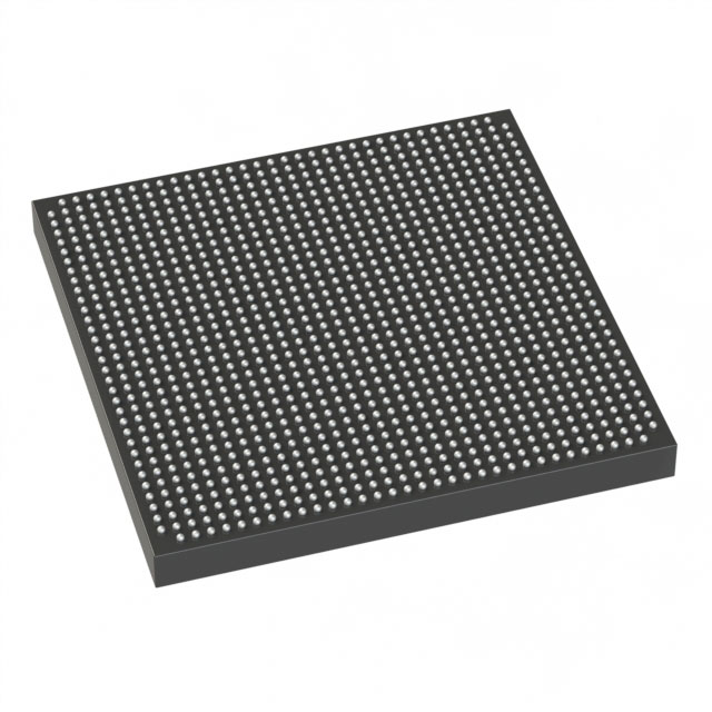
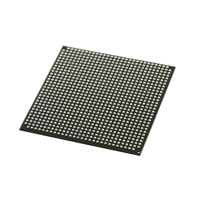
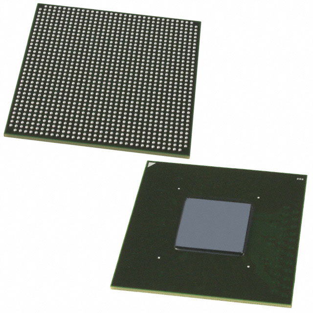
| Package / Case | 1152-BBGA, FCBGA | Number of I/O | 544 | Voltage | 1.07 V - 1.13 V | ||
| Mounting Method | Surface Mount | RoHS Compliance | RoHS Compliant | REACH Compliance | REACH Unaffected | ||
| Moisture Sensitivity Level | 3 (168 Hours) | Number of LABs/CLBs | 17110 | Number of Logic Elements/Cells | 362000 | ||
| Number of Gates | N/A | ECCN | PENDING ECCN | HTS Code | 0000.00.0000 | ||
| Qualification | N/A | Total RAM Bits | 19822592 |
Overview of 5AGXBB3D4F35C4G – Arria V GX Field Programmable Gate Array (FPGA) IC, 544 I/O, 1152-BBGA (FCBGA)
The Intel Arria V GX device 5AGXBB3D4F35C4G is a commercial-grade, high-density FPGA designed for systems that require large programmable logic capacity, substantial on-chip memory, and extensive external I/O. This surface-mount FCBGA package integrates 362,000 logic elements and approximately 19.8 Mbits of embedded RAM, enabling complex custom logic and data buffering on a single device.
Documented configuration and electrical specifications are provided in the Arria V device datasheet, including detailed operating conditions, configuration timing (JTAG, Active/Passive Serial, FPP), and I/O timing to support system design and integration.
Key Features
- Core Logic Capacity — 362,000 logic elements to implement large-scale custom logic and state machines.
- Embedded Memory — Approximately 19.8 Mbits of on-chip RAM for buffering, lookup tables, and small-cache functions.
- High I/O Count — 544 I/O pins to support wide external connectivity and parallel interfaces.
- Power and Voltage — Core supply voltage range specified at 1.07 V to 1.13 V for the device.
- Package and Mounting — 1152-BBGA, FCBGA (supplier package: 1152-FBGA, FC, 35×35 mm) optimized for surface-mount system integration.
- Operating Temperature — Commercial grade operation from 0 °C to 85 °C.
- Comprehensive Datasheet Coverage — Includes electrical characteristics, switching characteristics (transceiver and core), configuration specifications (POR, JTAG, AS, PS, FPP), and I/O timing to support design validation and system bring-up.
- RoHS Compliant — Conforms to RoHS environmental requirements.
Typical Applications
- High-density logic implementations — Leverage 362,000 logic elements for complex programmable logic arrays, signal processing pipelines, and custom state machines.
- I/O-intensive designs — Use 544 I/O pins to interface with multiple peripherals, parallel buses, or wide data paths requiring significant external connectivity.
- Embedded memory buffering — Take advantage of approximately 19.8 Mbits of on-chip RAM for packet buffering, frame buffering, or intermediate data storage.
- Platform and prototype integration — Surface-mount FCBGA package (35×35 mm) suitable for system-level integration and development platforms requiring a compact footprint.
Unique Advantages
- Highly integrated logic and memory — Combines 362,000 logic elements with ~19.8 Mbits of embedded RAM to reduce external component count and simplify board design.
- Extensive external connectivity — 544 I/O pins enable broad interface options without needing additional I/O expanders.
- Datasheet-backed configuration and timing — Complete configuration and timing documentation (POR, JTAG, Active/Passive Serial, FPP) supports reliable configuration and field upgrades.
- Commercial-grade thermal range — Rated for 0 °C to 85 °C operation to match a wide set of commercial electronics deployments.
- Industry-standard BGA package — 1152-BBGA FCBGA (35×35 mm) offers a standard mounting form factor for surface-mount manufacturing and system integration.
- Environmentally compliant — RoHS compliance supports regulatory requirements for lead-free assembly.
Why Choose 5AGXBB3D4F35C4G?
The 5AGXBB3D4F35C4G Arria V GX FPGA delivers a balanced combination of large programmable logic capacity, substantial on-chip RAM, and a very high I/O count in a single, surface-mount FCBGA package. It is well suited for commercial systems that require dense logic integration and broad external connectivity while relying on documented configuration and electrical specifications for system design.
Engineers and procurement teams benefit from Intel's detailed device datasheet that covers electrical characteristics, switching and core performance, and configuration timing—providing the technical foundation needed for robust integration and long-term platform support.
If you would like pricing or availability, request a quote or submit an inquiry to purchase this Intel Arria V GX FPGA.


Date Founded: 1968
Headquarters: Santa Clara, California, USA
Employees: 130,000+
Revenue: $54.23 Billion
Certifications and Memberships: ISO9001:2015, ISO14001:2015, ISO17025:2017, ISO27001:2022, ISO45001:2018, ISO50001:2018


