
5AGXBB3D4F31C5G
| Part Description |
Arria V GX Field Programmable Gate Array (FPGA) IC 384 19822592 362000 896-BBGA, FCBGA |
|---|---|
| Quantity | 1,856 Available (as of June 15, 2026) |

| Product Category | Field Programmable Gate Array (FPGA) |
|---|---|
| Manufacturer | Intel |
| Manufacturing Status | Active |
| Manufacturer Standard Lead Time | 12 Weeks |
| Datasheet |
Specifications & Environmental
| Device Package | 896-FBGA (31x31) | Grade | Commercial | Operating Temperature | 0°C – 85°C | ||
|---|---|---|---|---|---|---|---|
| Package / Case | 896-BBGA, FCBGA | Number of I/O | 384 | Voltage | 1.07 V - 1.13 V | ||
| Mounting Method | Surface Mount | RoHS Compliance | RoHS Compliant | REACH Compliance | REACH Unaffected | ||
| Moisture Sensitivity Level | 3 (168 Hours) | Number of LABs/CLBs | 17110 | Number of Logic Elements/Cells | 362000 | ||
| Number of Gates | N/A | ECCN | PENDING ECCN | HTS Code | 0000.00.0000 | ||
| Qualification | N/A | Total RAM Bits | 19822592 |
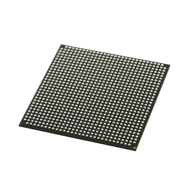
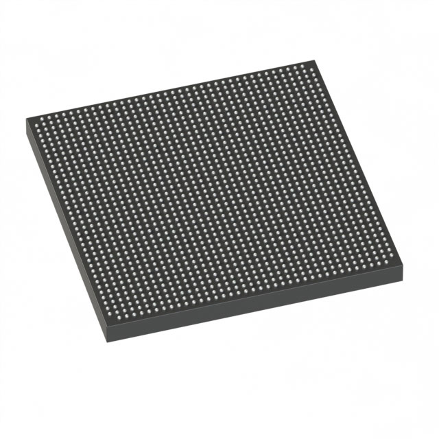
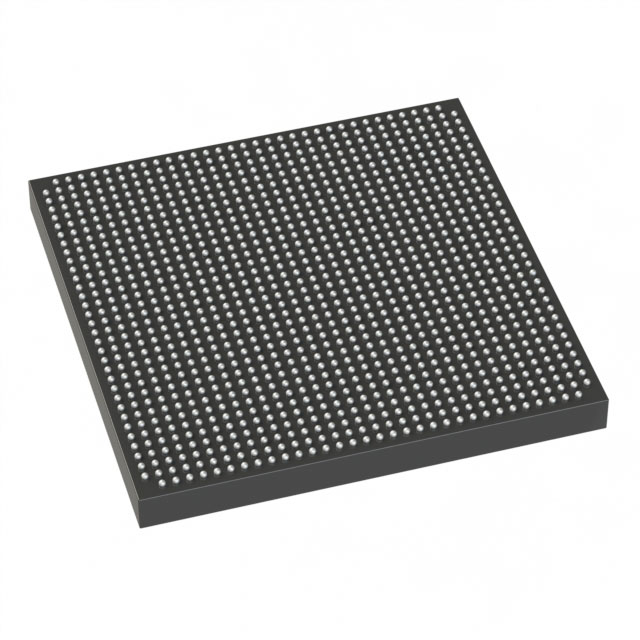
Overview of 5AGXBB3D4F31C5G – Arria V GX FPGA, 362,000 logic elements, ~19.8 Mbits RAM, 384 I/O, 896-BBGA
The 5AGXBB3D4F31C5G is an Arria V GX field programmable gate array (FPGA) IC offered in a commercial-grade device. It provides high logic capacity, substantial on-chip memory and a dense I/O complement in a 896‑ball BGA package for surface-mount integration.
Designed for programmable-logic applications that require large numbers of logic elements and embedded memory, this device offers a compact package footprint and a defined core supply voltage range, backed by the Arria V device datasheet for electrical and configuration specifications.
Key Features
- Logic Capacity 362,000 logic elements to implement complex, high-density digital designs.
- Embedded Memory Approximately 19.8 Mbits of on-chip RAM to support buffering, lookup tables, and data-path storage.
- I/O Density 384 user I/O pins for wide bus interfaces, parallel data paths, and mixed-signal front-end connectivity.
- Core Supply Voltage Operates with a core voltage supply range of 1.07 V to 1.13 V, facilitating defined power-rail design.
- Package & Mounting 896‑BBGA / FCBGA package (supplier device package listed as 896‑FBGA 31 × 31) with surface-mount mounting for compact board layouts.
- Operating Range Commercial grade with an operating temperature range from 0 °C to 85 °C for standard commercial applications.
- Compliance RoHS compliant for regulatory and assembly considerations.
Typical Applications
- High-density digital systems Implement large-scale programmable logic and control functions using the device’s significant logic and memory resources.
- Data-path buffering and processing Leverage the approximately 19.8 Mbits of embedded RAM for packet buffering, FIFOs, and intermediate data storage.
- Interface aggregation Use the 384 I/O pins to consolidate multiple parallel or serial interfaces on a single FPGA platform.
Unique Advantages
- Substantial logic resources: 362,000 logic elements enable consolidation of multiple functions and IP blocks into a single device, reducing board-level complexity.
- Integrated on-chip memory: Approximately 19.8 Mbits of embedded RAM reduces dependence on external memory and simplifies timing and layout for data-critical paths.
- High I/O count: 384 I/O pins provide flexibility for wide data buses, parallel interfaces, or mixed-signal front-end connectivity without additional glue logic.
- Compact BGA packaging: The 896‑ball BGA (31 × 31) package offers a high pin count in a space-efficient footprint suitable for dense PCB designs.
- Defined electrical envelope: Documented operating core voltage (1.07 V–1.13 V) and commercial temperature range simplify system power and thermal planning.
- Regulatory readiness: RoHS compliance supports modern manufacturing and environmental requirements.
Why Choose 5AGXBB3D4F31C5G?
The 5AGXBB3D4F31C5G Arria V GX FPGA combines a large logic fabric and significant embedded memory with a high I/O count in an industry-standard BGA package, making it well-suited for commercial systems that demand integrated programmable logic and dense connectivity. Its defined core voltage range and documented operating conditions (per the Arria V device datasheet) help streamline power delivery and system design considerations.
This device is ideal for developers and engineers building complex programmable designs who need a commercially graded FPGA with ample resources and a compact footprint, backed by detailed electrical and configuration specifications in the Arria V datasheet.
Request a quote or submit an inquiry to obtain pricing, availability, and additional technical support for the 5AGXBB3D4F31C5G Arria V GX FPGA.


Date Founded: 1968
Headquarters: Santa Clara, California, USA
Employees: 130,000+
Revenue: $54.23 Billion
Certifications and Memberships: ISO9001:2015, ISO14001:2015, ISO17025:2017, ISO27001:2022, ISO45001:2018, ISO50001:2018


