
5AGXFB1H4F40C5G
| Part Description |
Arria V GX Field Programmable Gate Array (FPGA) IC 704 17358848 300000 1517-BBGA, FCBGA |
|---|---|
| Quantity | 610 Available (as of June 15, 2026) |
| Product Category | Field Programmable Gate Array (FPGA) |
|---|---|
| Manufacturer | Intel |
| Manufacturing Status | Active |
| Manufacturer Standard Lead Time | 12 Weeks |
| Datasheet |
Specifications & Environmental
| Device Package | 1517-FBGA, FC (40x40) | Grade | Commercial | Operating Temperature | 0°C – 85°C | ||
|---|---|---|---|---|---|---|---|
| Package / Case | 1517-BBGA, FCBGA | Number of I/O | 704 | Voltage | 1.07 V - 1.13 V | ||
| Mounting Method | Surface Mount | RoHS Compliance | RoHS Compliant | REACH Compliance | REACH Unaffected | ||
| Moisture Sensitivity Level | 3 (168 Hours) | Number of LABs/CLBs | 14151 | Number of Logic Elements/Cells | 300000 | ||
| Number of Gates | N/A | ECCN | PENDING ECCN | HTS Code | 0000.00.0000 | ||
| Qualification | N/A | Total RAM Bits | 17358848 |
Overview of 5AGXFB1H4F40C5G – Arria V GX Field Programmable Gate Array (FPGA) IC
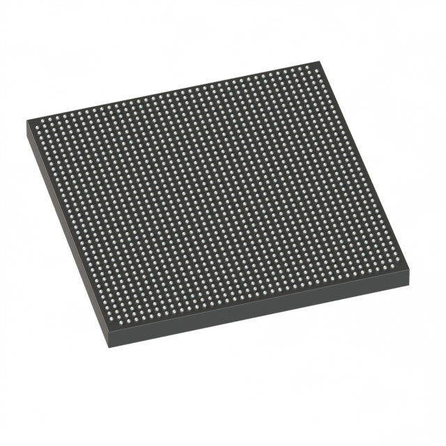
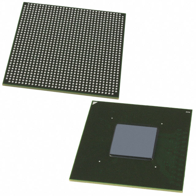
The 5AGXFB1H4F40C5G is an Intel Arria V GX family FPGA in a 1517-ball FCBGA package designed for commercial applications. It provides a large logic capacity and substantial embedded memory, combined with a high I/O count and surface-mount packaging for system integration.
Targeted at designs requiring up to 300,000 logic elements and approximately 17.36 Mbits of on-chip RAM, this device is well suited for complex digital designs where I/O density, embedded memory, and defined commercial temperature and voltage ranges are required.
Key Features
- Logic Capacity — 300,000 logic elements to implement large-scale digital designs and complex logic functions.
- Embedded Memory — Approximately 17.36 Mbits of total on-chip RAM for buffering, FIFOs, and intermediate storage.
- I/O Density — 704 user I/O pins to support extensive external interfacing and multi-channel connectivity.
- Package and Mounting — 1517-BBGA (FCBGA) package, supplier device package listed as 1517-FBGA, FC (40×40), in a surface-mount form factor for PCB assembly.
- Voltage Range — Core supply specified from 1.07 V to 1.13 V to match system power rails and design margins.
- Operating Grade and Temperature — Commercial grade with an operating temperature range of 0°C to 85°C.
- RoHS Compliant — Meets RoHS environmental requirements for lead-free design and manufacturing.
- Arria V Series Documentation — Series datasheet includes detailed electrical, switching, configuration, and I/O timing specifications for Arria V GX family devices.
Typical Applications
- High-density logic consolidation — Use the 300,000 logic elements to consolidate complex RTL and accelerate custom hardware functions.
- Memory-intensive processing — Leverage approximately 17.36 Mbits of on-chip RAM for buffering, packet queues, or lookup tables.
- I/O-rich system integration — 704 I/O pins support multi-channel interfaces, board-level peripherals, and dense connectivity requirements.
Unique Advantages
- Substantial logic resources: 300,000 logic elements provide headroom for feature-rich FPGA implementations without immediate migration.
- Significant on-chip RAM: Approximately 17.36 Mbits of embedded memory reduces reliance on external RAM for many buffering and storage needs.
- High I/O count: 704 I/O pins simplify routing for multi-interface designs and reduce the need for external multiplexing.
- Surface-mount FCBGA packaging: 1517-ball FCBGA (40×40) supports compact board layouts and standard assembly processes.
- Commercial temperature and power: Defined 0°C to 85°C operating temperature and 1.07 V–1.13 V core supply make system-level power and thermal planning straightforward.
- RoHS compliant: Facilitates integration into lead-free manufacturing workflows.
Why Choose 5AGXFB1H4F40C5G?
The 5AGXFB1H4F40C5G Arria V GX FPGA delivers a clear balance of logic density, embedded memory, and I/O capacity in a commercial-grade, surface-mount FCBGA package. Its specified voltage and temperature ranges, together with RoHS compliance, make it a practical choice for commercial products and prototypes that require sizable on-chip resources and extensive external interfacing.
Designers looking to implement complex digital functions with substantial local memory and broad I/O reach will find this device appropriate for consolidating functions, reducing external component count, and supporting scalable system designs backed by the Arria V family documentation.
Request a quote or submit a parts inquiry to get pricing, availability, and delivery details for 5AGXFB1H4F40C5G.


Date Founded: 1968
Headquarters: Santa Clara, California, USA
Employees: 130,000+
Revenue: $54.23 Billion
Certifications and Memberships: ISO9001:2015, ISO14001:2015, ISO17025:2017, ISO27001:2022, ISO45001:2018, ISO50001:2018


