
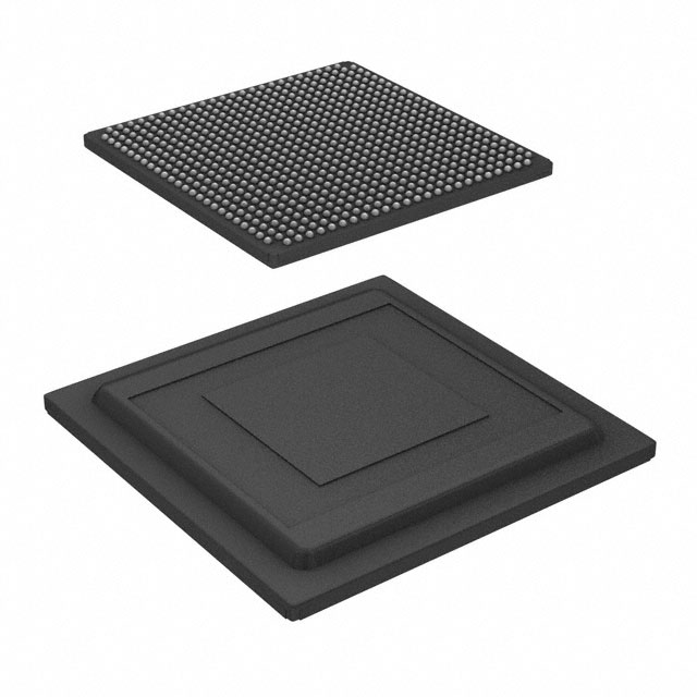
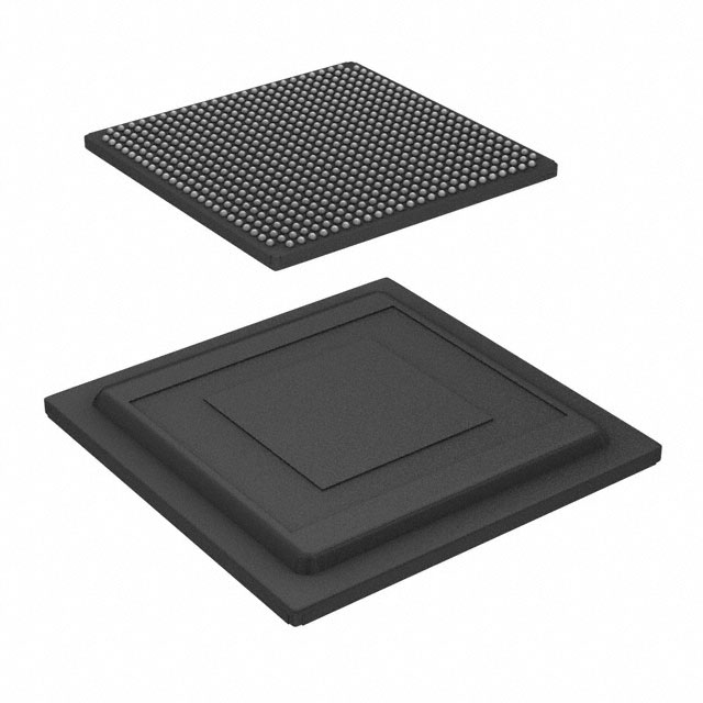
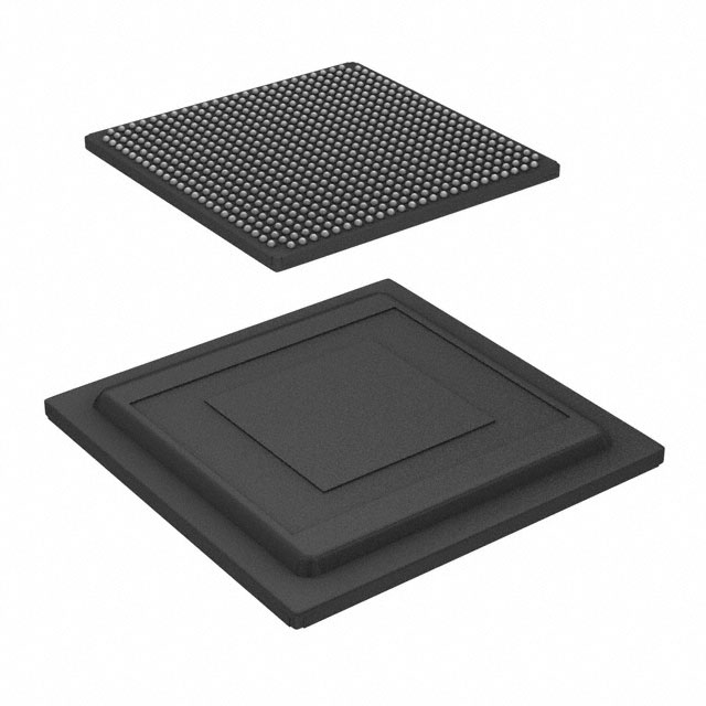
5AGXMA1D4F27C5G
| Part Description |
Arria V GX Field Programmable Gate Array (FPGA) IC 336 8666112 75000 672-BBGA, FCBGA |
|---|---|
| Quantity | 1,447 Available (as of October 8, 2026) |

| Product Category | Field Programmable Gate Array (FPGA) |
|---|---|
| Manufacturer | Intel |
| Manufacturing Status | Active |
| Manufacturer Standard Lead Time | 16 Weeks |
| Datasheet |
Specifications & Environmental
| Device Package | 672-FBGA (27x27) | Grade | Commercial | Operating Temperature | 0°C – 85°C | ||
|---|---|---|---|---|---|---|---|
| Package / Case | 672-BBGA, FCBGA | Number of I/O | 336 | Voltage | 1.07 V - 1.13 V | ||
| Mounting Method | Surface Mount | RoHS Compliance | RoHS Compliant | REACH Compliance | REACH Unaffected | ||
| Moisture Sensitivity Level | 3 (168 Hours) | Number of LABs/CLBs | 3537 | Number of Logic Elements/Cells | 75000 | ||
| Number of Gates | N/A | ECCN | PENDING ECCN | HTS Code | 0000.00.0000 | ||
| Qualification | N/A | Total RAM Bits | 8666112 |
Overview of 5AGXMA1D4F27C5G – Arria V GX FPGA, 75,000 Logic Elements, 672-BBGA (FCBGA)
The 5AGXMA1D4F27C5G is an Intel Arria V GX field‑programmable gate array delivered in a 672‑ball FCBGA package. It provides a high logic capacity FPGA fabric together with substantial on‑chip memory and a large I/O count for demanding programmable‑logic applications.
Designed for commercial‑grade systems, this device combines 75,000 logic elements, approximately 8.66 Mbits of embedded memory, and 336 user I/O pins in a 672‑FBGA (27×27) footprint, making it suitable where dense logic, local RAM, and numerous external interfaces are required.
Key Features
- Logic Capacity — 75,000 logic elements to implement complex digital designs and custom compute pipelines.
- Embedded Memory — Approximately 8.66 Mbits of on‑chip RAM to support buffering, lookup tables, and state storage without external memory.
- I/O Density — 336 user I/O pins for broad connectivity to peripherals, sensors, and high‑pin‑count interfaces.
- Logic Blocks — 3537 logic blocks reported for mapping and floorplanning reference.
- Power Envelope — Core supply operating range from 1.07 V to 1.13 V for predictable power budgeting and regulation design.
- Package & Mounting — 672‑ball BGA (FCBGA) 27×27 package, surface‑mountable for compact PCB implementations.
- Commercial Grade — Rated for 0 °C to 85 °C operation for typical commercial environments.
- Environmental Compliance — RoHS compliant for regulatory and manufacturing alignment.
Typical Applications
- Protocol Bridging & Interface Aggregation — Use the high I/O count and FPGA fabric to implement multi‑channel protocol adapters and interface translators.
- On‑chip Buffering & Packet Processing — Leverage the 8.66 Mbits of embedded RAM for packet buffering, FIFOs, and data staging in communication subsystems.
- Custom Compute & Acceleration — Map custom arithmetic or control logic across 75,000 logic elements to accelerate application‑specific workloads.
- High‑Density System Integration — The 672‑ball FCBGA package enables compact board layouts for space‑constrained designs requiring extensive I/O.
Unique Advantages
- Significant Logic Resources: 75,000 logic elements provide headroom for complex state machines, datapaths, and hardware accelerators.
- On‑Chip Memory: Approximately 8.66 Mbits of embedded RAM reduces dependency on external memory for latency‑sensitive buffering.
- Large I/O Count: 336 I/O pins simplify integration of multiple external devices and parallel interfaces without board-level multiplexing.
- Compact Packaging: 672‑FBGA (27×27) package delivers high integration density while remaining surface‑mount compatible for modern PCB assembly.
- Commercial Temperature Rating: Specified 0 °C to 85 °C operation for mainstream commercial applications and deployments.
- Regulatory Compatibility: RoHS compliance supports environmentally conscious manufacturing and supply chain requirements.
Why Choose 5AGXMA1D4F27C5G?
As a member of the Intel Arria V GX family, the 5AGXMA1D4F27C5G provides a balanced platform of logic capacity, embedded memory, and I/O real estate in a single commercial‑grade FPGA. Its combination of 75,000 logic elements, substantial on‑chip RAM, and 336 I/Os makes it well suited to designs that require dense programmable logic alongside significant local buffering and broad external connectivity.
This device is appropriate for engineers and teams building compact, high‑functionality systems who need a verified Arria V GX device in a 672‑ball FCBGA package with defined electrical and thermal operating limits for reliable integration into commercial products.
If you would like a quote or have questions about availability and lead time for 5AGXMA1D4F27C5G, submit a request and our team will provide pricing and purchasing options.






















Date Founded: 1968
Headquarters: Santa Clara, California, USA
Employees: 130,000+
Revenue: $54.23 Billion
Certifications and Memberships: ISO9001:2015, ISO14001:2015, ISO17025:2017, ISO27001:2022, ISO45001:2018, ISO50001:2018


