
5AGXMA1D4F27I3N
| Part Description |
Arria V GX Field Programmable Gate Array (FPGA) IC 336 8666112 75000 672-BBGA, FCBGA |
|---|---|
| Quantity | 754 Available (as of June 15, 2026) |
| Product Category | Field Programmable Gate Array (FPGA) |
|---|---|
| Manufacturer | Intel |
| Manufacturing Status | Obsolete |
| Manufacturer Standard Lead Time | Contact Us |
| Datasheet |
Specifications & Environmental
| Device Package | 672-FBGA (27x27) | Grade | Industrial | Operating Temperature | -40°C – 100°C | ||
|---|---|---|---|---|---|---|---|
| Package / Case | 672-BBGA, FCBGA | Number of I/O | 336 | Voltage | 1.12 V - 1.18 V | ||
| Mounting Method | Surface Mount | RoHS Compliance | RoHS Compliant | REACH Compliance | REACH Unknown | ||
| Moisture Sensitivity Level | 3 (168 Hours) | Number of LABs/CLBs | 3537 | Number of Logic Elements/Cells | 75000 | ||
| Number of Gates | N/A | ECCN | 3A001A2C | HTS Code | 8542.39.0001 | ||
| Qualification | N/A | Total RAM Bits | 8666112 |
Overview of 5AGXMA1D4F27I3N – Arria V GX FPGA, 75,000 logic elements, 336 I/O, 672‑BBGA
The 5AGXMA1D4F27I3N is an Arria V GX Field Programmable Gate Array (FPGA) IC from Intel. It integrates approximately 75,000 logic elements and roughly 8.67 Mbits of on‑chip RAM to support dense, configurable logic and memory requirements. With 336 I/O pins and industrial grade temperature support, this device is suited for FPGA‑based designs that require a combination of logic density, embedded memory, and a compact BGA package.
Key Features
- Logic Capacity Approximately 75,000 logic elements to implement complex programmable logic and custom datapaths.
- Embedded Memory Approximately 8.67 Mbits of on‑chip RAM (total RAM bits: 8,666,112) for buffering, FIFOs, and storage of intermediate data.
- I/O Density 336 user I/O pins enabling broad peripheral interfacing and parallel I/O requirements.
- Voltage Supply Core supply range: 1.12 V to 1.18 V to match platform power-rail requirements.
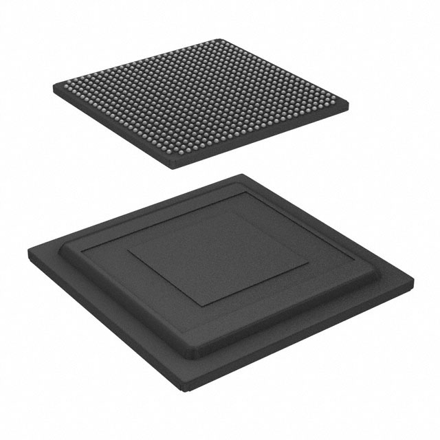
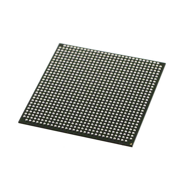
- Package & Mounting 672‑BBGA (FCBGA) package; supplier device package listed as 672‑FBGA (27×27). Surface mount construction for board‑level integration.
- Industrial Temperature Range Rated for operation from −40 °C to 100 °C, supporting industrial environments and extended thermal ranges.
- Compliance RoHS compliant, meeting common environmental requirements for electronic assemblies.
- Documentation Coverage Datasheet coverage includes electrical characteristics, switching characteristics, configuration specifications, and I/O timing for Arria V GX devices.
Typical Applications
- Industrial control and automation Industrial‑grade operating range and dense logic/memory resources support control logic, protocol handling, and deterministic I/O interfacing.
- FPGA development and prototyping Large logic element count and substantial on‑chip RAM make this device suitable for prototyping complex RTL designs and system integration tasks.
- High‑density I/O subsystems 336 I/O pins allow implementation of parallel interfaces, custom buses, and multiple peripheral connections on compact PCBs.
Unique Advantages
- Substantial configurable logic: The device’s approximately 75,000 logic elements enable implementation of large custom logic blocks and complex state machines without external glue logic.
- On‑chip memory capacity: Nearly 8.67 Mbits of embedded RAM reduces dependence on external memory for buffering and intermediate storage, simplifying board design.
- Robust I/O resources: 336 I/O pins provide flexibility for mixed parallel/serial interfacing and multiple peripheral connections in a single FPGA footprint.
- Industrial thermal rating: Operation from −40 °C to 100 °C supports deployment in harsh or temperature‑variable environments.
- Compact BGA packaging: 672‑ball FCBGA package (27×27) balances high pin count with a compact board footprint for space‑constrained designs.
- Standards‑oriented documentation: Detailed datasheet sections (electrical and switching characteristics, configuration timing, I/O timing) support accurate system integration and timing closure.
Why Choose 5AGXMA1D4F27I3N?
The 5AGXMA1D4F27I3N Arria V GX device combines substantial logic capacity and embedded memory with a high I/O count and industrial temperature rating, making it a practical choice for FPGA‑based subsystems where integration density and environmental robustness matter. Its 672‑BBGA package and defined core voltage range ease placement in compact, power‑managed designs.
This device is well suited to engineers and system designers looking for a scalable, well‑documented FPGA building block with verified electrical and configuration specifications for reliable system integration over the long term.
Request a quote or submit a purchasing inquiry to receive availability and pricing for 5AGXMA1D4F27I3N. Our team can provide order details and support to help you move from evaluation to production.


Date Founded: 1968
Headquarters: Santa Clara, California, USA
Employees: 130,000+
Revenue: $54.23 Billion
Certifications and Memberships: ISO9001:2015, ISO14001:2015, ISO17025:2017, ISO27001:2022, ISO45001:2018, ISO50001:2018


