
5AGXMA1D6F27C6G
| Part Description |
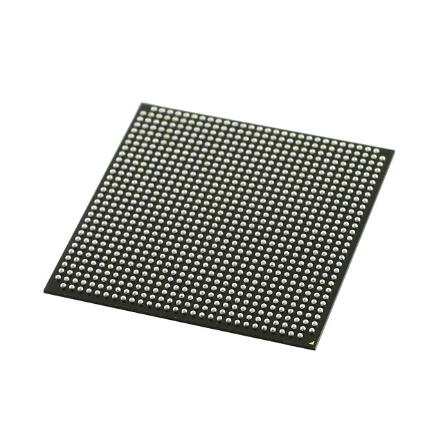
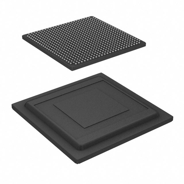
Arria V GX Field Programmable Gate Array (FPGA) IC 336 8666112 75000 672-BBGA, FCBGA |
|---|---|
| Quantity | 110 Available (as of June 15, 2026) |

| Product Category | Field Programmable Gate Array (FPGA) |
|---|---|
| Manufacturer | Intel |
| Manufacturing Status | Active |
| Manufacturer Standard Lead Time | 16 Weeks |
| Datasheet |
Specifications & Environmental
| Device Package | 672-FBGA (27x27) | Grade | Commercial | Operating Temperature | 0°C – 85°C | ||
|---|---|---|---|---|---|---|---|
| Package / Case | 672-BBGA, FCBGA | Number of I/O | 336 | Voltage | 1.07 V - 1.13 V | ||
| Mounting Method | Surface Mount | RoHS Compliance | RoHS Compliant | REACH Compliance | REACH Unaffected | ||
| Moisture Sensitivity Level | 3 (168 Hours) | Number of LABs/CLBs | 3537 | Number of Logic Elements/Cells | 75000 | ||
| Number of Gates | N/A | ECCN | PENDING ECCN | HTS Code | 0000.00.0000 | ||
| Qualification | N/A | Total RAM Bits | 8666112 |
Overview of 5AGXMA1D6F27C6G – Arria V GX FPGA, 75,000 Logic Elements, 336 I/Os, 672‑BBGA
The 5AGXMA1D6F27C6G is an Arria V GX Field Programmable Gate Array (FPGA) IC offered in a 672‑ball FCBGA package. It delivers a high logic capacity and embedded memory suitable for commercial-grade board designs that require dense I/O, substantial on‑chip RAM, and fine core voltage control.
Key attributes include approximately 75,000 logic elements, roughly 8.66 Mbits of embedded RAM, 336 user I/Os, and a specified core voltage supply range of 1.07 V to 1.13 V. The device is supplied in a surface‑mount 672‑FBGA (27×27) package and is RoHS compliant.
Key Features
- Logic Capacity Approximately 75,000 logic elements providing substantial programmable logic resources for complex designs.
- Embedded Memory Total on‑chip RAM of 8,666,112 bits (approximately 8.66 Mbits) to support buffering, FIFOs, and on‑chip data storage.
- I/O Density 336 user I/Os to support multi‑channel interfaces and high‑pin‑count connectivity on a single device.
- Power and Core Supply Specified core voltage range of 1.07 V to 1.13 V for controlled power provisioning and compatibility with precise power‑rail designs.
- Package and Mounting Surface‑mount 672‑BBGA (FCBGA) package; supplier device package listed as 672‑FBGA (27×27) for compact, high‑density board integration.
- Commercial Grade and Temperature Commercial grade device rated for operation from 0 °C to 85 °C for standard commercial embedded applications.
- Regulatory Compliance RoHS compliant to meet common environmental and lead‑free assembly requirements.
Typical Applications
- High‑density I/O systems Designs that require large numbers of external interfaces can leverage the 336 user I/Os to consolidate connectivity on a single FPGA.
- Memory‑intensive on‑chip processing Applications that need substantial on‑chip buffering or local data storage can take advantage of approximately 8.66 Mbits of embedded RAM.
- Compact board‑level FPGA integration The 672‑FBGA (27×27) surface‑mount package enables compact, high‑density PCB layouts for space‑constrained commercial products.
- Commercial embedded platforms Systems operating within 0 °C to 85 °C that require repeatable, commercially graded FPGA performance and RoHS compliance.
Unique Advantages
- Substantial logic resources: Approximately 75,000 logic elements allow implementation of complex custom logic, state machines, and compute blocks without partitioning across multiple devices.
- On‑chip memory capacity: Roughly 8.66 Mbits of embedded RAM reduces external memory dependence for many buffering and data‑flow tasks, simplifying board design.
- High I/O count: 336 user I/Os support multiple parallel interfaces and high‑pin‑count connectivity, minimizing the need for external multiplexing or additional FPGAs.
- Controlled core supply: A defined core voltage range (1.07 V–1.13 V) helps ensure predictable core power behavior and eases power‑supply design and validation.
- Compact surface‑mount package: The 672‑FBGA (27×27) package offers a balance of pin density and PCB area efficiency for commercial board assemblies.
- RoHS compliant: Meets lead‑free and environmental assembly requirements for commercial products.
Why Choose 5AGXMA1D6F27C6G?
The 5AGXMA1D6F27C6G Arria V GX FPGA provides a balanced combination of high logic capacity, substantial embedded RAM, and dense I/O in a compact 672‑BBGA surface‑mount package. Its specified core voltage range and commercial temperature rating make it appropriate for a wide range of commercial embedded designs that require predictable electrical characteristics and on‑chip resources.
This device is well suited to engineers and procurement teams building mid‑ to high‑complexity systems that benefit from integrated logic and memory, high connectivity, and RoHS compliance—delivering a platform that supports consolidation of functionality and streamlined board integration.
If you would like pricing, availability, or a formal quote for 5AGXMA1D6F27C6G, please submit a quote request or product inquiry and our team will respond with the next steps.


Date Founded: 1968
Headquarters: Santa Clara, California, USA
Employees: 130,000+
Revenue: $54.23 Billion
Certifications and Memberships: ISO9001:2015, ISO14001:2015, ISO17025:2017, ISO27001:2022, ISO45001:2018, ISO50001:2018


