
5AGXMA5D6F27C6G
| Part Description |
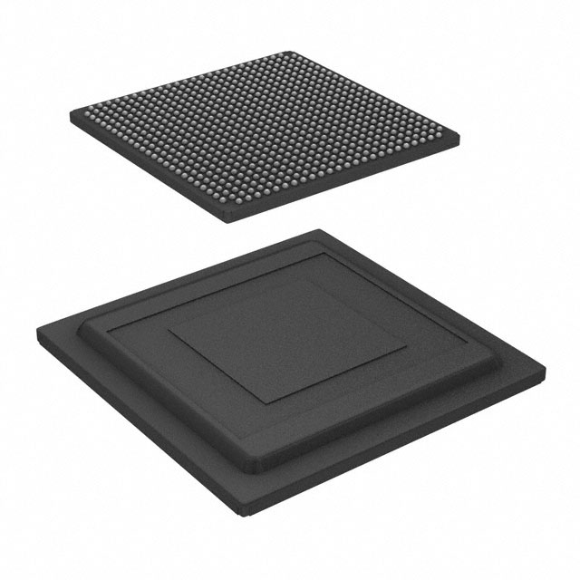
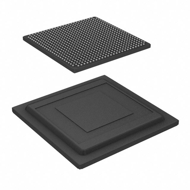
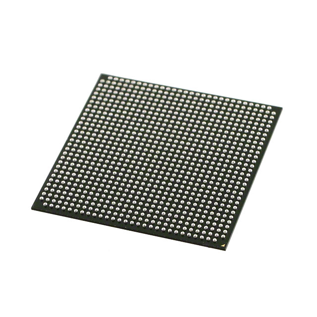
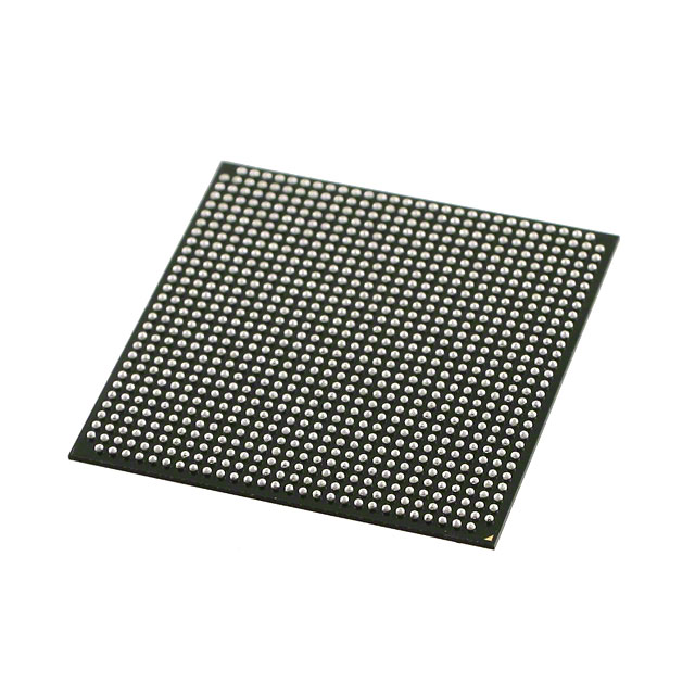
Arria V GX Field Programmable Gate Array (FPGA) IC 336 13284352 190000 672-BBGA, FCBGA |
|---|---|
| Quantity | 226 Available (as of October 8, 2026) |

| Product Category | Field Programmable Gate Array (FPGA) |
|---|---|
| Manufacturer | Intel |
| Manufacturing Status | Active |
| Manufacturer Standard Lead Time | 12 Weeks |
| Datasheet |
Specifications & Environmental
| Device Package | 672-FBGA (27x27) | Grade | Commercial | Operating Temperature | 0°C – 85°C | ||
|---|---|---|---|---|---|---|---|
| Package / Case | 672-BBGA, FCBGA | Number of I/O | 336 | Voltage | 1.07 V - 1.13 V | ||
| Mounting Method | Surface Mount | RoHS Compliance | RoHS Compliant | REACH Compliance | REACH Unaffected | ||
| Moisture Sensitivity Level | 3 (168 Hours) | Number of LABs/CLBs | 8962 | Number of Logic Elements/Cells | 190000 | ||
| Number of Gates | N/A | ECCN | PENDING ECCN | HTS Code | 0000.00.0000 | ||
| Qualification | N/A | Total RAM Bits | 13284352 |
Overview of 5AGXMA5D6F27C6G – Arria V GX FPGA, 190,000 logic elements, ~13.28 Mbits RAM, 336 I/Os, 672-FBGA
The 5AGXMA5D6F27C6G is an Arria V GX Field Programmable Gate Array (FPGA) IC offering high logic density and substantial on-chip memory in a compact FCBGA package. Built for commercial-grade applications, this device combines a large number of logic elements, abundant embedded RAM, and a high I/O count to support complex system designs.
With a nominal core supply range of 1.07 V to 1.13 V and an operating temperature range of 0 °C to 85 °C, this device is specified for commercial deployments that require dense programmable logic, flexible I/O, and surface-mount packaging.
Key Features
- Logic Capacity — 190,000 logic elements provide extensive programmable logic resources for complex combinational and sequential designs.
- Embedded Memory — Approximately 13.28 Mbits of on-chip RAM to support data buffering, FIFOs, and local storage for high-throughput logic.
- I/O Resources — 336 user I/Os to enable broad peripheral, bus, and system interfacing options.
- Package — 672-ball FCBGA packaging (supplier device package: 672-FBGA, 27×27) optimized for high-density board integration; surface-mount mounting type.
- Power — Core supply specified from 1.07 V to 1.13 V to match system power-rail planning and decoupling strategies.
- Operating Conditions — Commercial grade with an ambient operating temperature range of 0 °C to 85 °C and RoHS compliance for regulatory conformance.
- Comprehensive Device Documentation — The Arria V device family documentation includes detailed electrical characteristics, switching and transceiver performance specifications, configuration timing, and I/O timing to support system design and integration.
Typical Applications
- High-density digital systems — Use the large logic element count and embedded RAM for custom digital processing, control logic, and state-machine implementations.
- Data-path buffering and bridging — On-chip RAM and abundant I/O support local buffering, protocol bridging, and interface adaptation between subsystems.
- Prototyping and system integration — Compact FCBGA packaging and surface-mount mounting make the device suitable for tightly integrated prototype and production boards in commercial products.
Unique Advantages
- High logic density: 190,000 logic elements allow implementation of complex algorithms and large-scale glue logic without external programmable devices.
- Significant embedded memory: Approximately 13.28 Mbits of on-chip RAM reduces the need for external RAM in many data-path and buffering applications.
- Extensive I/O count: 336 I/Os provide flexibility for multi-channel interfaces, parallel buses, and numerous peripheral connections.
- Compact, manufacturable package: 672-ball FCBGA (27×27) supports dense PCB layouts and standard surface-mount assembly processes.
- Commercial-grade specification: Specified operating temperature and RoHS compliance align with mainstream commercial product requirements.
- Documented performance and configuration: Detailed Arria V family datasheet content covers electrical, switching, transceiver, and configuration specifications to aid engineering validation and system-level design.
Why Choose 5AGXMA5D6F27C6G?
The 5AGXMA5D6F27C6G Arria V GX FPGA delivers a balance of high logic capacity, on-chip memory, and extensive I/O in a compact FCBGA package targeted at commercial applications. Its documented electrical and configuration specifications support disciplined system design and help accelerate integration into production hardware.
This device is well suited for engineers and designers developing complex digital systems that require significant programmable logic and embedded RAM while maintaining a surface-mount form factor and commercial operating profile.
Request a quote or submit a product inquiry to receive pricing, lead-time, and availability information for the 5AGXMA5D6F27C6G Arria V GX FPGA.




















Date Founded: 1968
Headquarters: Santa Clara, California, USA
Employees: 130,000+
Revenue: $54.23 Billion
Certifications and Memberships: ISO9001:2015, ISO14001:2015, ISO17025:2017, ISO27001:2022, ISO45001:2018, ISO50001:2018


