
5CEFA9F27C8N
| Part Description |
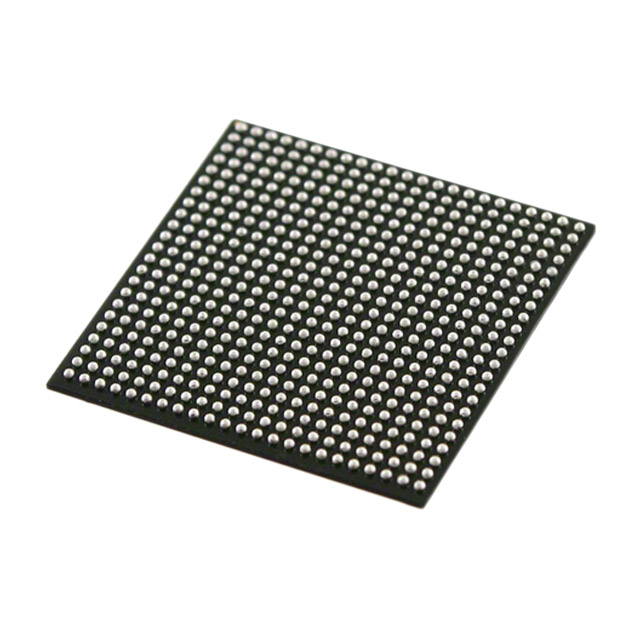
Cyclone® V E Field Programmable Gate Array (FPGA) IC 336 14251008 301000 672-BGA |
|---|---|
| Quantity | 553 Available (as of June 15, 2026) |

| Product Category | Field Programmable Gate Array (FPGA) |
|---|---|
| Manufacturer | Intel |
| Manufacturing Status | Active |
| Manufacturer Standard Lead Time | 16 Weeks |
| Datasheet |
Specifications & Environmental
| Device Package | 672-FBGA (27x27) | Grade | Commercial | Operating Temperature | 0°C – 85°C | ||
|---|---|---|---|---|---|---|---|
| Package / Case | 672-BGA | Number of I/O | 336 | Voltage | 1.07 V - 1.13 V | ||
| Mounting Method | Surface Mount | RoHS Compliance | RoHS Compliant | REACH Compliance | REACH Unaffected | ||
| Moisture Sensitivity Level | 3 (168 Hours) | Number of LABs/CLBs | 113560 | Number of Logic Elements/Cells | 301000 | ||
| Number of Gates | N/A | ECCN | 3A991D | HTS Code | 8542.39.0001 | ||
| Qualification | N/A | Total RAM Bits | 14251008 |
Overview of 5CEFA9F27C8N – Cyclone® V E FPGA, 301,000 Logic Elements, 672-BGA
The 5CEFA9F27C8N is a Cyclone® V E field programmable gate array offered in a 672-ball BGA (27 × 27) package. It integrates 301,000 logic elements and approximately 14.25 Mbits of embedded memory to address cost-sensitive, performance-oriented designs requiring high logic density and on-chip memory.
Targeted for commercial applications, this device supports up to 336 I/O signals, operates from a core supply range of 1.07 V to 1.13 V, and is specified for 0 °C to 85 °C. The Cyclone V family features low-power 28 nm technology and architecture elements designed for flexible logic, DSP, and memory integration.
Key Features
- Logic Capacity 301,000 logic elements, enabling substantial programmable logic for complex control, signal processing, and glue-logic functions.
- Embedded Memory Approximately 14.25 Mbits of on-chip RAM to support buffering, lookup tables, and local data storage for accelerated processing.
- I/O and Package 336 user I/O pins presented in a 672-BGA (672-FBGA, 27 × 27 mm) package for dense board-level integration and flexible interfacing.
- Core Voltage Designed to run from a narrow core supply range of 1.07 V to 1.13 V (nominal 1.1 V), consistent with low-power process operation.
- Commercial Temperature Grade Specified for 0 °C to 85 °C operation for standard commercial deployments.
- Low-Power 28 nm Technology Cyclone V family devices are built on a 28 nm low-power process and include architecture features such as 8-input adaptive logic modules and variable-precision DSP blocks to balance performance with efficiency.
- On-chip Memory Blocks Family-level memory architecture includes M10K memory blocks with ECC support, enabling reliable embedded storage and error detection capabilities.
- Standards & Compliance RoHS-compliant, supporting regulatory requirements for lead-free manufacturing processes.
Typical Applications
- Wireless and Wireline Communications Use the device’s logic density and on-chip memory to implement protocol processing, packet buffering, and interface bridging in communications equipment.
- Embedded Processing & Acceleration Leverage the combination of large logic fabric and embedded RAM for data-path acceleration, DSP functions, and custom co-processing in SoC designs.
- High-density I/O Control With 336 I/O pins in a compact 672-BGA package, the device is suitable for applications requiring many system interfaces such as sensor aggregation and board-level glue logic.
Unique Advantages
- Substantial On-chip Resources: 301,000 logic elements and approximately 14.25 Mbits of embedded memory provide headroom for large finite-state machines, datapaths, and buffering without external RAM.
- Compact, High-pin Package: The 672-FBGA (27 × 27) package packs 336 usable I/Os for dense system integration while keeping board area efficient.
- Low-voltage Core Operation: A narrow 1.07 V–1.13 V core supply window aligns with low-power design goals and helps simplify power-supply design for the FPGA fabric.
- Architecture Optimized for Mixed Tasks: Family features such as 8-input adaptive logic modules and variable-precision DSP blocks enable flexible mapping of control, signal-processing, and arithmetic workloads.
- Regulatory Ready: RoHS compliance supports lead-free manufacturing and global environmental requirements.
Why Choose 5CEFA9F27C8N?
The 5CEFA9F27C8N balances high logic density, substantial embedded memory, and a compact BGA footprint to address commercial designs that require integrated logic and memory without excessive board-level complexity. Its narrow core-voltage range and 28 nm family architecture provide a pragmatic combination of power efficiency and programmable capability.
This device is well suited to engineers building communication front-ends, embedded accelerators, or high-I/O control systems who need a commercially graded FPGA with clear, verifiable specifications for core voltage, operating temperature, I/O count, and package type.
Request a quote or submit a purchase inquiry to evaluate 5CEFA9F27C8N for your next FPGA-based design.


Date Founded: 1968
Headquarters: Santa Clara, California, USA
Employees: 130,000+
Revenue: $54.23 Billion
Certifications and Memberships: ISO9001:2015, ISO14001:2015, ISO17025:2017, ISO27001:2022, ISO45001:2018, ISO50001:2018


