
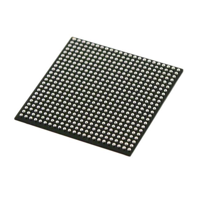
5CEFA9F23C8N
| Part Description |
Cyclone® V E Field Programmable Gate Array (FPGA) IC 224 14251008 301000 484-BGA |
|---|---|
| Quantity | 1,191 Available (as of June 10, 2026) |

| Product Category | Field Programmable Gate Array (FPGA) |
|---|---|
| Manufacturer | Intel |
| Manufacturing Status | Active |
| Manufacturer Standard Lead Time | 16 Weeks |
| Datasheet |
Specifications & Environmental
| Device Package | 484-FBGA (23x23) | Grade | Commercial | Operating Temperature | 0°C – 85°C | ||
|---|---|---|---|---|---|---|---|
| Package / Case | 484-BGA | Number of I/O | 224 | Voltage | 1.07 V - 1.13 V | ||
| Mounting Method | Surface Mount | RoHS Compliance | RoHS Compliant | REACH Compliance | REACH Unaffected | ||
| Moisture Sensitivity Level | 3 (168 Hours) | Number of LABs/CLBs | 113560 | Number of Logic Elements/Cells | 301000 | ||
| Number of Gates | N/A | ECCN | 3A991D | HTS Code | 8542.39.0001 | ||
| Qualification | N/A | Total RAM Bits | 14251008 |
Overview of 5CEFA9F23C8N – Cyclone® V E FPGA, 301,000 Logic Elements, 484‑BGA
The 5CEFA9F23C8N is an Intel Cyclone® V E field programmable gate array (FPGA) supplied in a 484‑FBGA (23×23) package. Built for cost- and power‑sensitive designs, this device combines a high logic capacity with substantial on‑chip memory and a rich I/O complement to support communication and embedded-processor-centric systems.
Targeted markets include industrial and wireless/wireline applications where integration, low core voltage operation, and a compact BGA footprint help reduce board complexity and system cost.
Key Features
- Logic Capacity — 301,000 logic elements and approximately 113,560 adaptive logic modules (ALMs) for implementing complex digital functions and custom logic.
- Embedded Memory — Approximately 13.6 Mbits of on‑chip RAM (total RAM bits: 14,251,008) to support buffering, packet processing, and on‑chip data storage.
- I/O and Package — 224 user I/Os in a 484‑FBGA (23×23) surface‑mount package (484‑BGA), enabling dense board routing and high‑pin count connectivity.
- Power — Core voltage supply range of 1.07 V to 1.13 V, supporting low‑power system designs.
- Operating Range & Grade — Commercial grade device rated for 0 °C to 85 °C operation.
- Integration & IP — Cyclone V family features include 8‑input adaptive logic modules, variable‑precision DSP blocks, hard memory controllers, and integrated transceiver options as described in the Cyclone V device documentation.
- Compliance — RoHS‑compliant manufacturing status.
Typical Applications
- Wireless and Wireline Communications — FPGA fabric, embedded memory, and transceiver-enabled architecture support protocol processing, packet handling, and interface bridging.
- Industrial Control and Automation — Compact BGA footprint and substantial logic/memory resources enable motor control, sensor interfacing, and programmable I/O aggregation.
- Embedded SoC and Processing — The Cyclone V family’s embedded processing features and hard IP are suitable for offloading compute tasks and accelerating application‑specific functions.
Unique Advantages
- High Logic Density: 301,000 logic elements provide headroom for complex custom logic and system integration on a single device.
- Significant On‑Chip Memory: Approximately 13.6 Mbits of embedded RAM reduce external memory dependency and improve throughput for buffering and packet processing.
- Low‑Voltage Core Operation: 1.07 V to 1.13 V core supply supports lower power consumption in system designs.
- Compact, High‑Pin Package: 484‑FBGA (23×23) surface‑mount package with 224 I/Os enables dense PCB implementations without sacrificing connectivity.
- RoHS Compliant: Meets RoHS requirements for lead‑free manufacturing and global regulatory needs.
- Designed for Integration: Cyclone V family features such as adaptive logic modules, DSP blocks, and hard memory controllers simplify system architecture and reduce bill‑of‑materials.
Why Choose 5CEFA9F23C8N?
This Cyclone V E FPGA balances large logic and memory resources with a compact 484‑BGA footprint and low core voltage operation, making it suitable for designs that demand integration without excessive board area or power. Its commercial operating range, RoHS compliance, and extensive on‑chip resources make it a practical choice for communications, industrial control, and embedded processing applications.
Engineers seeking to consolidate multiple board components into a single programmable device will find the 5CEFA9F23C8N offers a practical combination of capacity, connectivity (224 I/Os), and on‑chip memory to accelerate time‑to‑market while controlling system cost.
Request a quote or submit an inquiry to receive pricing and availability for the 5CEFA9F23C8N. Include your target quantities and any required procurement details to expedite the response.


Date Founded: 1968
Headquarters: Santa Clara, California, USA
Employees: 130,000+
Revenue: $54.23 Billion
Certifications and Memberships: ISO9001:2015, ISO14001:2015, ISO17025:2017, ISO27001:2022, ISO45001:2018, ISO50001:2018


