
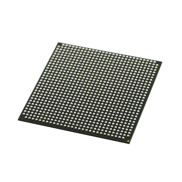
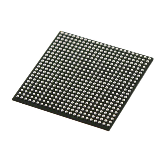
5CGXFC7D6F27C6N
| Part Description |
Cyclone® V GX Field Programmable Gate Array (FPGA) IC 336 7880704 149500 672-BGA |
|---|---|
| Quantity | 510 Available (as of June 19, 2026) |

| Product Category | Field Programmable Gate Array (FPGA) |
|---|---|
| Manufacturer | Intel |
| Manufacturing Status | Active |
| Manufacturer Standard Lead Time | 16 Weeks |
| Datasheet |
Specifications & Environmental
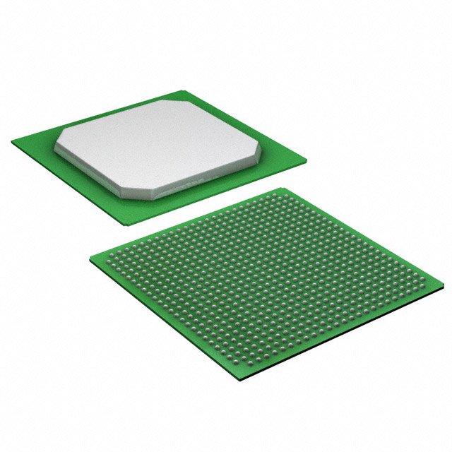
| Device Package | 672-FBGA (27x27) | Grade | Commercial | Operating Temperature | 0°C – 85°C | ||
|---|---|---|---|---|---|---|---|
| Package / Case | 672-BGA | Number of I/O | 336 | Voltage | 1.07 V - 1.13 V | ||
| Mounting Method | Surface Mount | RoHS Compliance | RoHS Compliant | REACH Compliance | REACH Unaffected | ||
| Moisture Sensitivity Level | 3 (168 Hours) | Number of LABs/CLBs | 56480 | Number of Logic Elements/Cells | 149500 | ||
| Number of Gates | N/A | ECCN | 3A001A7A | HTS Code | 8542.39.0001 | ||
| Qualification | N/A | Total RAM Bits | 7880704 |
Overview of 5CGXFC7D6F27C6N – Cyclone® V GX Field Programmable Gate Array (FPGA) IC 336 7880704 149500 672-BGA
The 5CGXFC7D6F27C6N is an Intel Cyclone® V GX FPGA in a 672-BGA (27 × 27 mm) package. It delivers a high-density programmable fabric with approximately 149,500 logic elements and integrated high-speed resources for bandwidth‑sensitive embedded designs.
Targeted at commercial applications in industrial, wireless and wireline, and military markets, this device combines a 28 nm low-power process architecture with integrated transceivers and hard memory controllers to balance performance, power efficiency, and system integration.
Key Features
- Logic Capacity Approximately 149,500 logic elements provide substantial programmable fabric for complex control, signal processing, and custom logic implementations.
- Embedded Memory Approximately 7.88 Mbits of on-chip RAM to support buffering, frame storage, and local data structures.
- I/O Count 336 user I/Os to connect to peripherals, memories, and high-density system interfaces.
- High-speed Transceivers Integrated transceivers (family-level capability) to support high bandwidth serial links for wireless and wireline applications.
- DSP and Logic Architecture Enhanced 8-input adaptive logic modules and variable-precision DSP blocks (family-level features) for efficient implementation of arithmetic and signal-processing functions.
- Process and Power Built on TSMC 28 nm low-power (28LP) process technology with a nominal core voltage around 1.1 V and specified supply range of 1.07 V to 1.13 V for stable low-voltage operation.
- Package & Mounting 672‑FBGA (27 × 27 mm) surface-mount package suitable for automated PCB assembly and high-density board designs.
- Operating Range Commercial grade operation from 0 °C to 85 °C and RoHS-compliant packaging.
Typical Applications
- Wireless Infrastructure Baseband and front-end processing where integrated transceivers and DSP resources accelerate protocol and signal tasks.
- Wireline Networking Line cards and packet-processing subsystems that require programmable logic, on-chip RAM buffering, and numerous I/Os.
- Industrial Control Real-time control, motor drive interfaces, and sensor aggregation leveraging dense logic and on-chip memory for deterministic processing.
- Military Systems Communications and signal-processing subsystems that benefit from programmable algorithms and high-speed serial links (suitability based on product family positioning).
Unique Advantages
- High programmable density: Large logic capacity supports complex custom logic, control paths, and multi-function designs within a single device.
- Integrated bandwidth features: On-chip transceivers and memory controllers reduce external component count and simplify high-throughput system design.
- Low-voltage operation: Narrow supply range around 1.1 V supports low-power system designs and aligns with 28 nm low-power process characteristics.
- Balanced memory and DSP resources: Approximately 7.88 Mbits of embedded RAM plus variable-precision DSP blocks enable efficient implementation of buffering and compute-heavy functions.
- Commercial-grade reliability: Specified commercial operating temperature range and RoHS compliance for mainstream embedded and communication products.
Why Choose 5CGXFC7D6F27C6N?
This Cyclone V GX device is positioned for designers who need substantial programmable logic, integrated high-speed interfaces, and on-chip memory in a compact BGA package. It offers a balance of performance and power economy derived from the 28 nm low-power process and a focused set of system-level features suited to industrial, wireless/wireline, and military applications.
For projects that require scalable logic density, numerous I/Os, and embedded RAM for data buffering and processing, 5CGXFC7D6F27C6N provides a verified platform with family-level enhancements—helping reduce system complexity and component count while enabling faster time to market.
Request a quote or submit an inquiry for 5CGXFC7D6F27C6N to receive pricing and availability information tailored to your production needs.


Date Founded: 1968
Headquarters: Santa Clara, California, USA
Employees: 130,000+
Revenue: $54.23 Billion
Certifications and Memberships: ISO9001:2015, ISO14001:2015, ISO17025:2017, ISO27001:2022, ISO45001:2018, ISO50001:2018


