
5CGXFC9A6U19C7N
| Part Description |
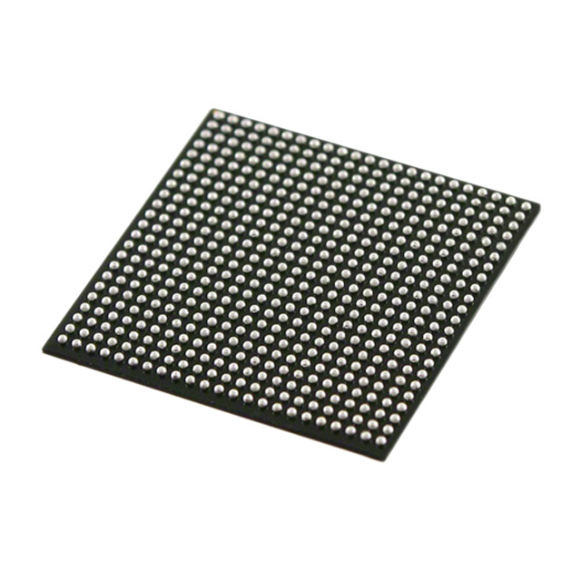
Cyclone® V GX Field Programmable Gate Array (FPGA) IC 240 14251008 301000 484-FBGA |
|---|---|
| Quantity | 206 Available (as of June 18, 2026) |

| Product Category | Field Programmable Gate Array (FPGA) |
|---|---|
| Manufacturer | Intel |
| Manufacturing Status | Active |
| Manufacturer Standard Lead Time | 16 Weeks |
| Datasheet |
Specifications & Environmental
| Device Package | 484-UBGA (19x19) | Grade | Commercial | Operating Temperature | 0°C – 85°C | ||
|---|---|---|---|---|---|---|---|
| Package / Case | 484-FBGA | Number of I/O | 240 | Voltage | 1.07 V - 1.13 V | ||
| Mounting Method | Surface Mount | RoHS Compliance | RoHS Compliant | REACH Compliance | REACH Unaffected | ||
| Moisture Sensitivity Level | 3 (168 Hours) | Number of LABs/CLBs | 113560 | Number of Logic Elements/Cells | 301000 | ||
| Number of Gates | N/A | ECCN | 3A001A2C | HTS Code | 8542.39.0001 | ||
| Qualification | N/A | Total RAM Bits | 14251008 |
Overview of 5CGXFC9A6U19C7N – Cyclone® V GX FPGA, 301,000 Logic Elements, 240 I/O, 484‑FBGA
The 5CGXFC9A6U19C7N is a Cyclone® V GX field programmable gate array (FPGA) in a 484‑FBGA package that delivers high logic density and embedded memory for cost‑sensitive, bandwidth‑driven designs. It integrates a large programmable fabric with on‑chip memory and signal I/O to address applications in industrial, wireless and wireline, and military systems.
Designed as part of the Cyclone V family, this device emphasizes efficient power and system integration while providing the logic, memory, and I/O resources needed for mid‑to‑high complexity FPGA designs.
Key Features
- High Logic Capacity — 301,000 logic elements to implement complex digital functions and custom accelerators.
- Embedded Memory — Approximately 14.25 Mbits of on‑chip RAM for buffering, FIFOs, and storage of intermediate data.
- I/O Resources — 240 general purpose I/O pins to interface with a wide range of peripherals and external devices.
- Process and Core Voltage — Built on TSMC 28‑nm low‑power (28LP) technology with a core supply range of 1.07 V to 1.13 V for optimized power-performance tradeoffs.
- Integrated System Features — Cyclone V devices are enhanced with integrated transceivers and hard memory controllers to support higher bandwidth external interfaces (as described in Cyclone V family documentation).
- Package and Mounting — Supplied in a 484‑FBGA (supplier package: 484‑UBGA, 19×19) surface‑mount package for compact board integration.
- Operating Conditions — Commercial grade operation from 0 °C to 85 °C with RoHS compliance for regulatory conformance.
Typical Applications
- Industrial Control — Motor control, PLC I/O aggregation, and deterministic logic functions leveraging the device’s large logic capacity and on‑chip memory.
- Wireless and Wireline Infrastructure — Packet buffering, packet processing, and protocol bridging using abundant RAM and high I/O counts.
- Military and Ruggedized Systems — Embedded processing and custom signal processing blocks where reconfigurable logic and memory are required (within commercial temperature range constraints).
Unique Advantages
- High integration density: 301,000 logic elements reduce the need for multiple discrete components and simplify board-level design.
- Substantial embedded memory: Approximately 14.25 Mbits of on‑chip RAM enables local data storage and reduces external memory bandwidth requirements.
- Generous I/O count: 240 I/Os allow flexible interfacing to sensors, peripherals, and external memory devices.
- Low‑voltage core operation: Narrow core supply range (1.07 V–1.13 V) supports efficient power provisioning and predictable power budgeting.
- Compact, surface‑mount packaging: 484‑FBGA (484‑UBGA, 19×19) offers a balanced footprint for space-constrained boards.
- RoHS compliant: Environmentally compliant manufacturing supports global production requirements.
Why Choose 5CGXFC9A6U19C7N?
The 5CGXFC9A6U19C7N positions itself as a scalable, high‑density FPGA option within the Cyclone V GX family, combining a significant logic element count with multi‑Mbit embedded RAM and a large I/O complement. Its 28‑nm low‑power heritage and defined core voltage range make it appropriate for designs that prioritize a balance of performance, integration, and power efficiency.
This device is well suited for engineers and procurement teams building mid‑to‑high complexity systems in industrial, wireless/wireline, and military application spaces who need a reconfigurable platform with substantial on‑chip resources and a compact BGA package.
If you require pricing, availability, or lead‑time information, request a quote or submit a pricing inquiry to receive a prompt response.


Date Founded: 1968
Headquarters: Santa Clara, California, USA
Employees: 130,000+
Revenue: $54.23 Billion
Certifications and Memberships: ISO9001:2015, ISO14001:2015, ISO17025:2017, ISO27001:2022, ISO45001:2018, ISO50001:2018


