
5CGXFC7D7F31C8N
| Part Description |
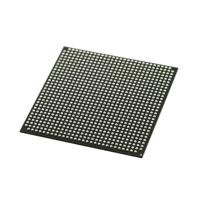
Cyclone® V GX Field Programmable Gate Array (FPGA) IC 480 7880704 149500 896-BGA |
|---|---|
| Quantity | 1,177 Available (as of June 9, 2026) |

| Product Category | Field Programmable Gate Array (FPGA) |
|---|---|
| Manufacturer | Intel |
| Manufacturing Status | Active |
| Manufacturer Standard Lead Time | 16 Weeks |
| Datasheet |
Specifications & Environmental
| Device Package | 896-FBGA (31x31) | Grade | Commercial | Operating Temperature | 0°C – 85°C | ||
|---|---|---|---|---|---|---|---|
| Package / Case | 896-BGA | Number of I/O | 480 | Voltage | 1.07 V - 1.13 V | ||
| Mounting Method | Surface Mount | RoHS Compliance | RoHS Compliant | REACH Compliance | REACH Unaffected | ||
| Moisture Sensitivity Level | 3 (168 Hours) | Number of LABs/CLBs | 56480 | Number of Logic Elements/Cells | 149500 | ||
| Number of Gates | N/A | ECCN | 3A991D | HTS Code | 8542.39.0001 | ||
| Qualification | N/A | Total RAM Bits | 7880704 |
Overview of 5CGXFC7D7F31C8N – Cyclone V GX FPGA, 896‑BGA
The 5CGXFC7D7F31C8N is an Intel Cyclone V GX field‑programmable gate array provided in an 896‑BGA (896‑FBGA, 31×31) package. This commercial‑grade FPGA combines a high logic capacity with substantial on‑chip RAM and a dense I/O count for embedded designs that require integration of logic, memory, and high‑speed interfaces.
Built on a 28‑nm low‑power process with a nominal 1.1 V core, the device addresses applications in wireless and wireline communications, industrial systems, and defense equipment that benefit from programmable hardware, integrated transceivers, and on‑chip memory and controllers.
Key Features
- Logic Capacity — 149,500 logic elements for complex programmable logic and custom datapath implementation.
- Embedded Memory — Approximately 7.88 Mbits of on‑chip RAM to support buffering, FIFOs, and local storage for high‑throughput designs.
- I/O Density — 480 I/O pins to accommodate multiple peripherals, bus interfaces, and external memory connections.
- Process and Core Voltage — Manufactured on TSMC 28‑nm low‑power (28LP) technology with a supply range of 1.07 V to 1.13 V for core power.
- Package and Mounting — 896‑pin BGA (896‑FBGA, 31×31) in a surface‑mount form factor for board‑level integration.
- Operating Conditions — Commercial grade with an operating temperature range of 0 °C to 85 °C.
- Compliance — RoHS‑compliant material status.
- Integrated Architecture — Cyclone V GX family features such as integrated transceivers and hard memory controllers (as described in device family documentation) to support high‑bandwidth interfaces and memory subsystems.
Typical Applications
- Wireless Infrastructure — Programmable logic and on‑chip RAM provide flexible packet processing, framing, and interface handling for base station subsystems.
- Wireline Communications — Dense I/O and embedded memory enable protocol handling, buffering, and interface bridging in access and aggregation equipment.
- Industrial Systems — Use for motor control, sensor aggregation, and custom I/O processing where high logic capacity and plentiful I/O are required.
- Defense and Aerospace Subsystems — High logic element count and embedded memory support real‑time signal processing and custom control logic for mission electronics.
Unique Advantages
- High Logic Density: 149,500 logic elements allow implementation of complex algorithms and parallel datapaths on a single device, reducing board count.
- Substantial On‑Chip RAM: Approximately 7.88 Mbits of embedded memory reduces reliance on external RAM for buffering and accelerates data‑path performance.
- Large I/O Complement: 480 I/Os support multiple peripheral interfaces and wide external memory buses without extensive multiplexing.
- Low Core Voltage Operation: Nominal 1.1 V operation (1.07–1.13 V range) aligns with low‑power system designs and modern power architectures.
- Compact BGA Package: 896‑FBGA (31×31) offers a high pin count in a compact surface‑mount footprint for space‑constrained applications.
- RoHS Compliant: Meets RoHS requirements for environmentally conscious manufacturing and assembly processes.
Why Choose 5CGXFC7D7F31C8N?
The 5CGXFC7D7F31C8N delivers a balanced combination of high logic capacity, significant embedded memory, and abundant I/O in a compact BGA package—making it well suited for designs that require programmable hardware acceleration, flexible protocol handling, and tight board‑level integration. Its 28‑nm low‑power process and defined core voltage range support efficient power delivery and predictable thermal design within commercial operating conditions.
This part is a strong fit for engineering teams building communication equipment, embedded controllers, and high‑throughput data paths that need scalable FPGA capability combined with on‑chip memory and interface integration backed by Cyclone V family documentation and ecosystem resources.
Request a quote or submit an inquiry to receive pricing, lead time, and availability for the 5CGXFC7D7F31C8N. Our team can provide technical details and assist with integration planning for your design.


Date Founded: 1968
Headquarters: Santa Clara, California, USA
Employees: 130,000+
Revenue: $54.23 Billion
Certifications and Memberships: ISO9001:2015, ISO14001:2015, ISO17025:2017, ISO27001:2022, ISO45001:2018, ISO50001:2018


