
5SGSED6K3F40C3N
| Part Description |
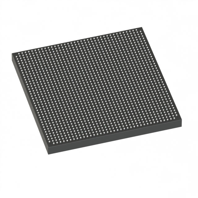
Stratix® V GS Field Programmable Gate Array (FPGA) IC 696 46080000 583000 1517-BBGA, FCBGA |
|---|---|
| Quantity | 386 Available (as of June 15, 2026) |

| Product Category | Field Programmable Gate Array (FPGA) |
|---|---|
| Manufacturer | Intel |
| Manufacturing Status | Obsolete |
| Manufacturer Standard Lead Time | Contact Us |
| Datasheet |
Specifications & Environmental
| Device Package | 1517-FBGA (40x40) | Grade | Commercial | Operating Temperature | 0°C – 85°C | ||
|---|---|---|---|---|---|---|---|
| Package / Case | 1517-BBGA, FCBGA | Number of I/O | 696 | Voltage | 820 mV - 880 mV | ||
| Mounting Method | Surface Mount | RoHS Compliance | RoHS Compliant | REACH Compliance | REACH Unknown | ||
| Moisture Sensitivity Level | 3 (168 Hours) | Number of LABs/CLBs | 220000 | Number of Logic Elements/Cells | 583000 | ||
| Number of Gates | N/A | ECCN | 3A001A2C | HTS Code | 8542.39.0001 | ||
| Qualification | N/A | Total RAM Bits | 46080000 |
Overview of 5SGSED6K3F40C3N – Stratix® V GS Field Programmable Gate Array (FPGA) IC 696 I/O, ~46 Mbits RAM, 583000 logic elements, 1517-BBGA
The 5SGSED6K3F40C3N is an Intel Stratix V GS FPGA configured for DSP-centric, transceiver-enabled designs. Built on the Stratix V family architecture, it delivers a combination of large logic capacity, substantial on-chip memory, and integrated transceiver and DSP resources suited for bandwidth- and compute-intensive applications.
This device provides approximately 583,000 logic elements, about 46 Mbits of embedded memory, and 696 I/O pins in a 1517-BBGA FCBGA package, making it appropriate for high-density signal processing, networking, and communications systems operating within commercial temperature and voltage ranges.
Key Features
- Logic Capacity Approximately 583,000 logic elements for complex FPGA designs and high gate-count implementations.
- Embedded Memory Approximately 46 Mbits of on-chip RAM (total RAM bits: 46,080,000) to support large buffering, packet processing, and on-chip data storage.
- DSP Resources Stratix V GS family devices include abundant variable-precision DSP blocks; the family supports high-density multiplier configurations suitable for high-performance signal processing workloads.
- Integrated Transceivers GS-series devices provide integrated transceivers with multi-gigabit data-rate capability for backplane, optical, and high-speed serial interfaces.
- I/O and Packaging 696 I/O pins in a 1517-BBGA (supplier device package: 1517-FBGA, 40×40) surface-mount package, enabling dense board connectivity and flexible I/O mapping.
- Power and Temperature Core supply range specified at 820 mV to 880 mV with commercial-grade operating temperature from 0 °C to 85 °C, matching typical commercial system requirements.
- Fabric and Clocking Stratix V devices use an enhanced core architecture with multi-track routing and comprehensive fabric clocking, plus fractional PLLs for flexible clock management and timing control.
- Design Integration The family includes embedded hard IP blocks such as the Embedded HardCopy Block for hardened PCIe instantiation and other system-level IP integration.
- RoHS Compliant Device is RoHS compliant for environmental and manufacturing requirements.
Typical Applications
- High-performance Digital Signal Processing Use the device’s dense DSP resources and large on-chip memory for waveform processing, FFTs, and algorithmic acceleration in broadcast and compute systems.
- Network and Optical Transport Integrated transceivers and abundant logic make this FPGA suitable for packet processing, backplane interfaces, and 40G/100G optical transport system elements.
- Military and Broadcast Systems The combination of DSP capability and multi-gigabit transceivers supports real-time signal handling and high-throughput streaming in communications and broadcast equipment.
- High-performance Computing (HPC) Acceleration Large logic and memory resources enable implementation of custom acceleration kernels and data-path engines for compute-intensive workloads.
Unique Advantages
- High Logic Density: Approximately 583,000 logic elements allow integration of complex state machines, protocol stacks, and datapath logic on a single device, reducing board-level component count.
- Substantial On-chip Memory: About 46 Mbits of embedded RAM supports large buffers and reduces external memory dependence for many real-time and packet-processing applications.
- Extensive I/O Availability: 696 I/O pins in a 1517-BBGA package provide flexible I/O mapping for multi-channel systems and dense peripheral connectivity.
- Transceiver and DSP Integration: On-die transceivers and variable-precision DSP blocks simplify high-bandwidth and signal-processing designs by consolidating critical functions into the FPGA fabric.
- Commercial-grade Compatibility: Specified for 0 °C to 85 °C operation and RoHS compliance to meet common commercial manufacturing and deployment requirements.
- Power-optimized Core Range: Core voltage range of 820 mV to 880 mV enables designs that target low-voltage FPGA cores consistent with family-level power architectures.
Why Choose 5SGSED6K3F40C3N?
The 5SGSED6K3F40C3N offers a balanced combination of large logic capacity, significant embedded memory, rich DSP resources, and integrated transceiver capability in a compact 1517-BBGA package. Its Stratix V GS-class architecture targets transceiver-based, DSP-heavy applications where on-chip compute and high-speed I/O are central to system performance.
This device is well suited for engineering teams building high-throughput networking, communications, broadcast, and compute-acceleration solutions that require integrated DSP and serial interfaces while operating within commercial voltage and temperature ranges. The Stratix V family architecture and embedded hard IP also support design reuse and migration paths for production scaling.
Request a quote or submit a purchase inquiry for part number 5SGSED6K3F40C3N to receive pricing, availability, and ordering information.


Date Founded: 1968
Headquarters: Santa Clara, California, USA
Employees: 130,000+
Revenue: $54.23 Billion
Certifications and Memberships: ISO9001:2015, ISO14001:2015, ISO17025:2017, ISO27001:2022, ISO45001:2018, ISO50001:2018


