
5SGSED6K3F40C2LN
| Part Description |
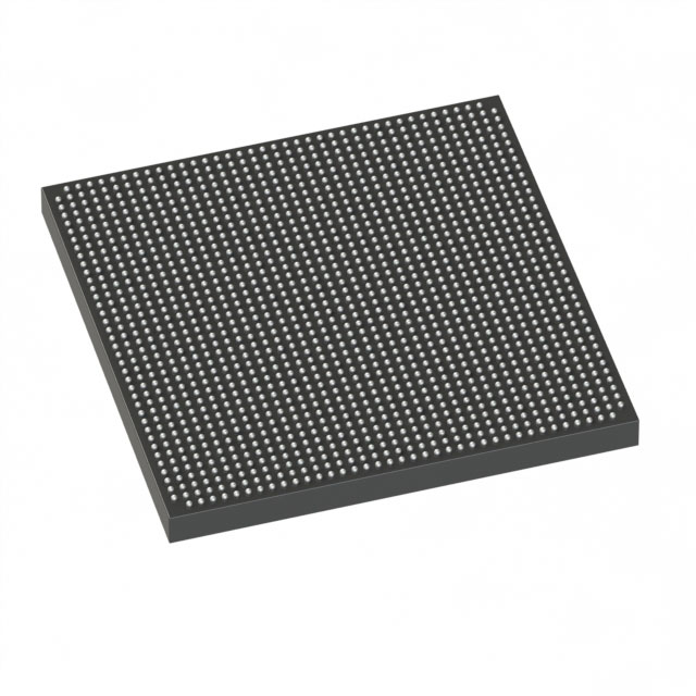
Stratix® V GS Field Programmable Gate Array (FPGA) IC 696 46080000 583000 1517-BBGA, FCBGA |
|---|---|
| Quantity | 752 Available (as of June 10, 2026) |
| Product Category | Field Programmable Gate Array (FPGA) |
|---|---|
| Manufacturer | Intel |
| Manufacturing Status | Obsolete |
| Manufacturer Standard Lead Time | Contact Us |
| Datasheet |
Specifications & Environmental
| Device Package | 1517-FBGA (40x40) | Grade | Commercial | Operating Temperature | 0°C – 85°C | ||
|---|---|---|---|---|---|---|---|
| Package / Case | 1517-BBGA, FCBGA | Number of I/O | 696 | Voltage | 820 mV - 880 mV | ||
| Mounting Method | Surface Mount | RoHS Compliance | RoHS Compliant | REACH Compliance | REACH Unknown | ||
| Moisture Sensitivity Level | 3 (168 Hours) | Number of LABs/CLBs | 220000 | Number of Logic Elements/Cells | 583000 | ||
| Number of Gates | N/A | ECCN | 3A001A2C | HTS Code | 8542.39.0001 | ||
| Qualification | N/A | Total RAM Bits | 46080000 |
Overview of 5SGSED6K3F40C2LN – Stratix® V GS FPGA, 583000 logic elements, ~46 Mbits RAM, 696 I/Os, 1517-BBGA
The 5SGSED6K3F40C2LN is a Stratix V GS field-programmable gate array (FPGA) offered in a 1517-BBGA FCBGA package. It combines a high-density logic fabric with abundant embedded memory and DSP resources targeted at transceiver-based, DSP-centric applications.
Designed for bandwidth- and compute-intensive designs, this commercial-grade device delivers a balance of logic capacity, on-chip RAM, and high I/O count to support demanding signal processing, networking, and compute acceleration tasks.
Key Features
- Core architecture Stratix V family architecture based on a 28‑nm process with embedded hard IP blocks and an adaptive logic module fabric.
- Logic capacity 583,000 logic elements to implement large, complex designs and wide datapaths.
- Embedded memory Approximately 46 Mbits of on-chip RAM (total RAM bits: 46,080,000) for buffering, packet processing, and intermediate data storage.
- DSP and transceiver capabilities GS-class devices provide an abundance of variable-precision DSP blocks; the Stratix V family documentation notes support for high-count multipliers (for example, up to 3,926 18×18 or 1,963 27×27 multipliers in GS devices) and integrated transceivers suitable for backplane and optical interfaces.
- I/O and connectivity 696 user I/Os to accommodate high-pin-count interfaces and parallel/serial connectivity requirements.
- Power and voltage Device core supply range specified at 820 mV to 880 mV; Stratix V family references 0.85‑V or 0.9‑V core options as part of the device architecture.
- Package and mounting 1517‑BBGA (FCBGA) package, supplier package listed as 1517‑FBGA (40×40), surface-mount mounting for PCB assembly.
- Operating range and grade Commercial grade with an operating temperature range of 0 °C to 85 °C.
- Environmental compliance RoHS compliant.
Typical Applications
- High-performance digital signal processing Variable-precision DSP blocks and large logic capacity support complex filtering, FFTs, and other high-throughput signal processing workloads.
- Optical and backplane communications Integrated transceiver capabilities and high I/O count suit 40G/100G class transport and packet-processing line cards.
- Compute acceleration Dense logic and on-chip RAM enable hardware acceleration of algorithms for high-performance computing and broadcast processing.
Unique Advantages
- High-density programmable fabric: 583,000 logic elements provide the capacity to implement large-scale, custom hardware functions without immediate ASIC transition.
- Substantial on-chip RAM: Approximately 46 Mbits of embedded memory reduces external memory dependence and accelerates data-path operations.
- DSP-optimized resources: GS-class DSP block availability supports wide-ranging multiplier configurations for precision-flexible signal processing.
- Extensive I/O: 696 I/Os allow integration of multiple high-speed interfaces and wide parallel buses on a single device.
- Compact BGA package: 1517‑BBGA FCBGA surface-mount package offers a high pin-count footprint for dense PCB designs.
- Standards-aware family features: Stratix V family includes integrated hard IP (such as PCIe hard blocks referenced in family documentation) and multi-track routing architecture to streamline system-level design.
Why Choose 5SGSED6K3F40C2LN?
The 5SGSED6K3F40C2LN positions itself as a high-capacity, DSP-focused FPGA for commercial applications that demand large logic density, significant on-chip memory, and broad I/O capability. Its Stratix V GS heritage brings family-level features—such as variable-precision DSP resources and integrated transceiver technology—useful for signal-intensive and high-bandwidth designs.
This device is well suited to teams building advanced networking, broadcast, and compute-acceleration hardware who need a scalable, field-programmable platform with commercial temperature range and RoHS compliance.
Request a quote or submit an inquiry to receive pricing, availability, and lead-time information for part number 5SGSED6K3F40C2LN.


Date Founded: 1968
Headquarters: Santa Clara, California, USA
Employees: 130,000+
Revenue: $54.23 Billion
Certifications and Memberships: ISO9001:2015, ISO14001:2015, ISO17025:2017, ISO27001:2022, ISO45001:2018, ISO50001:2018


