
5SGSED8N2F45I3N
| Part Description |
Stratix® V GS Field Programmable Gate Array (FPGA) IC 840 51200000 695000 1932-BBGA, FCBGA |
|---|---|
| Quantity | 289 Available (as of June 15, 2026) |
| Product Category | Field Programmable Gate Array (FPGA) |
|---|---|
| Manufacturer | Intel |
| Manufacturing Status | Obsolete |
| Manufacturer Standard Lead Time | Contact Us |
| Datasheet |
Specifications & Environmental
| Device Package | 1932-FBGA, FC (45x45) | Grade | Industrial | Operating Temperature | -40°C – 100°C | ||
|---|---|---|---|---|---|---|---|
| Package / Case | 1932-BBGA, FCBGA | Number of I/O | 840 | Voltage | 820 mV - 880 mV | ||
| Mounting Method | Surface Mount | RoHS Compliance | RoHS Compliant | REACH Compliance | REACH Unknown | ||
| Moisture Sensitivity Level | 3 (168 Hours) | Number of LABs/CLBs | 262400 | Number of Logic Elements/Cells | 695000 | ||
| Number of Gates | N/A | ECCN | 3A001A2C | HTS Code | 8542.39.0001 | ||
| Qualification | N/A | Total RAM Bits | 51200000 |
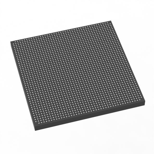
Overview of 5SGSED8N2F45I3N – Stratix® V GS FPGA, 840 I/Os, ~51.2 Mbits RAM, 695,000 logic elements, 1932-BBGA FCBGA
The 5SGSED8N2F45I3N is a Stratix® V GS Field Programmable Gate Array (FPGA) in a 1932-BBGA FCBGA package. It delivers high on-chip capacity with 695,000 logic elements and approximately 51.2 Mbits of embedded RAM, along with a large 840‑pin I/O complement.
Specified for industrial operation and designed for surface-mount assembly, this device targets designs that require substantial programmable logic density, significant embedded memory, and a high I/O count within a 45×45 supplier package footprint. Electrical and switching characteristics for the Stratix V family are documented in the Stratix V device datasheet.
Key Features
- Core capacity Approximately 695,000 logic elements to support complex programmable logic and large-scale integration on a single device.
- Embedded memory Approximately 51.2 Mbits of on-chip RAM for buffering, state storage, and memory-intensive logic functions.
- I/O resources 840 user I/Os for broad external connectivity and interfacing to high-pin-count systems.
- Package and mounting 1932-BBGA FCBGA supplier package (1932-FBGA, FC 45×45) with surface-mount mounting type for compact board-level integration.
- Power supply Core voltage range specified from 820 mV to 880 mV to align with the device’s power requirements.
- Temperature and grade Industrial grade with an operating temperature range of −40°C to 100°C for deployment in temperature-demanding environments.
- Regulatory RoHS compliant.
Typical Applications
- High-density programmable logic Large-scale designs that require extensive logic resources and embedded memory can consolidate functions onto this device.
- High I/O systems Systems needing broad external connectivity and multi‑lane interfacing benefit from the 840 available I/Os.
- Industrial equipment Industrial-grade temperature range makes the device suitable for applications that operate between −40°C and 100°C.
Unique Advantages
- High logic integration: The device’s ~695,000 logic elements enable consolidation of complex functions into a single FPGA, reducing board-level partitioning.
- Substantial on-chip memory: Approximately 51.2 Mbits of embedded RAM supports large buffers, LUT-based storage, and memory-hungry algorithms without immediate reliance on external memory.
- Extensive I/O resources: 840 user I/Os provide flexibility for wide parallel interfaces, multiple peripheral connections, and high-pin-count system designs.
- Industrial temperature rating: Specified operating range of −40°C to 100°C supports deployment in temperature-challenging environments.
- Compact FCBGA package: 1932-BBGA / 1932-FBGA (45×45) package supports high pin density in a board-space efficient form factor for surface-mount assembly.
- Low-voltage core: Core supply range of 820–880 mV aligns with modern low-voltage FPGA power domains.
Why Choose 5SGSED8N2F45I3N?
The 5SGSED8N2F45I3N combines extensive logic capacity, substantial embedded memory, and a high I/O count in a compact 1932‑BBGA FCBGA package. Its industrial temperature rating and RoHS compliance make it suitable for demanding deployments where on-chip resources and reliability matter.
This device is well suited for engineering teams and procurement groups building high-density programmable logic systems that require consolidated functionality, large on-chip storage, and broad connectivity while maintaining a surface-mount board-level footprint.
Request a quote or submit an inquiry to obtain pricing, availability, and additional technical support information for 5SGSED8N2F45I3N.


Date Founded: 1968
Headquarters: Santa Clara, California, USA
Employees: 130,000+
Revenue: $54.23 Billion
Certifications and Memberships: ISO9001:2015, ISO14001:2015, ISO17025:2017, ISO27001:2022, ISO45001:2018, ISO50001:2018


