
5SGSMD4H2F35I2N
| Part Description |
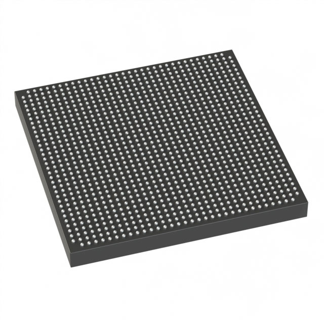
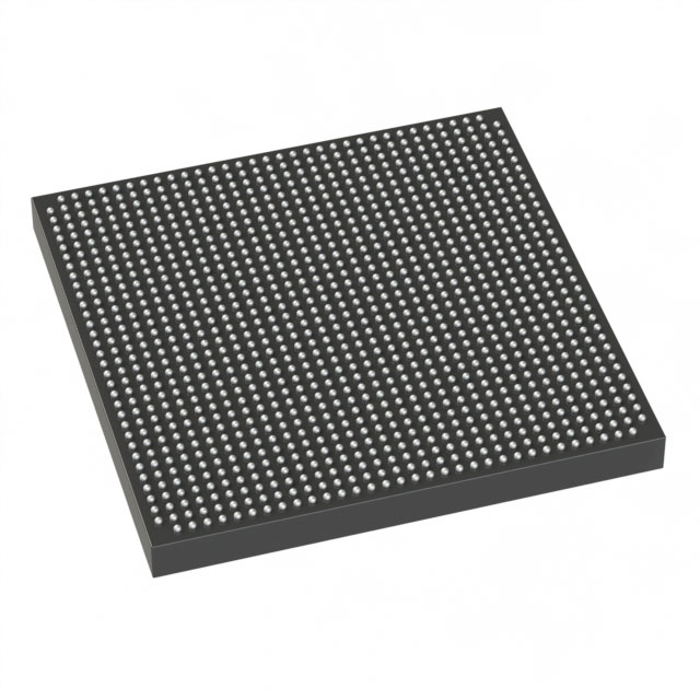
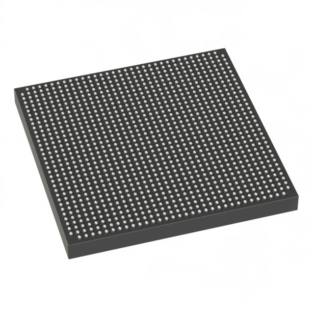
Stratix® V GS Field Programmable Gate Array (FPGA) IC 432 19456000 360000 1152-BBGA, FCBGA |
|---|---|
| Quantity | 1,053 Available (as of October 7, 2026) |
| Product Category | Field Programmable Gate Array (FPGA) |
|---|---|
| Manufacturer | Intel |
| Manufacturing Status | Obsolete |
| Manufacturer Standard Lead Time | Contact Us |
| Datasheet |
Specifications & Environmental
| Device Package | 1152-FBGA (35x35) | Grade | Industrial | Operating Temperature | -40°C – 100°C | ||
|---|---|---|---|---|---|---|---|
| Package / Case | 1152-BBGA, FCBGA | Number of I/O | 432 | Voltage | 870 mV - 930 mV | ||
| Mounting Method | Surface Mount | RoHS Compliance | RoHS Compliant | REACH Compliance | REACH Unknown | ||
| Moisture Sensitivity Level | 3 (168 Hours) | Number of LABs/CLBs | 135840 | Number of Logic Elements/Cells | 360000 | ||
| Number of Gates | N/A | ECCN | 3A001A2C | HTS Code | 8542.39.0001 | ||
| Qualification | N/A | Total RAM Bits | 19456000 |
Overview of 5SGSMD4H2F35I2N – Stratix® V GS FPGA, 360000 logic elements, 1152‑BBGA
The 5SGSMD4H2F35I2N is an Intel Stratix V GS field-programmable gate array (FPGA) in a 1152-BBGA (1152-FBGA, 35×35) package. It implements a 28-nm Stratix V architecture with an emphasis on high-precision DSP capability and integrated transceivers for bandwidth‑centric, transceiver‑based designs.
This industrial‑grade device combines large logic capacity, substantial on‑chip memory, and high I/O count to support data‑intensive applications such as wireline communications, broadcast and military communications systems, and high‑performance computing.
Key Features
- Logic Capacity 360,000 logic elements for implementing large, complex digital designs.
- Embedded Memory Approximately 19.456 Mbits of on‑chip RAM to support buffering, FIFOs, and large data structures.
- DSP Resources Stratix V GS family devices provide an abundance of variable‑precision DSP blocks (family documentation cites support for up to 3,926 18×18 or 1,963 27×27 multipliers), enabling high‑throughput signal processing implementations.
- High‑Speed Transceivers Integrated transceivers with 14.1 Gbps capability (Stratix V GS family), suitable for backplane and optical interface applications.
- I/O and Integration 432 I/O pins to connect to high‑bandwidth peripherals and system interfaces.
- Process and Core Built on 28‑nm TSMC process technology with enhanced core architecture and integrated hard IP blocks for functions such as PCIe Gen3 (family‑level features documented in the Stratix V device overview).
- Power Core voltage range specified at 870 mV to 930 mV.
- Package and Mounting 1152‑BBGA (1152‑FBGA, 35×35) surface‑mount package for high‑density board integration.
- Operating Range Industrial operating temperature range from −40 °C to 100 °C.
- RoHS Compliance Device RoHS status: Compliant.
Typical Applications
- Wireline Communications Transceiver and DSP resources support backplane and optical transport functions in high‑bandwidth network equipment.
- Broadcast and Military Communications Variable‑precision DSP blocks and high‑speed I/O enable real‑time signal processing and interface handling for broadcast and defense systems.
- High‑Performance Computing Large logic capacity and substantial on‑chip memory support compute‑intensive acceleration and data‑path implementations.
- Data‑Intensive Networking Integrated transceivers and abundant logic make the device suitable for 40G/100G class networking and other bandwidth‑centric protocols.
Unique Advantages
- High Logic Density: 360,000 logic elements provide the capacity to implement complex control, routing, and processing functions on a single device.
- Substantial On‑Chip Memory: Approximately 19.456 Mbits of embedded RAM reduces external memory dependency for buffering and packet handling.
- Rich DSP Resources: Family‑level variable‑precision DSP blocks enable efficient implementation of high‑precision signal processing algorithms.
- Integrated High‑Speed Transceivers: 14.1‑Gbps capable transceivers (Stratix V GS family) simplify implementation of high‑bandwidth serial links.
- Industrial Temperature Rating: −40 °C to 100 °C operating range supports deployment in demanding environments.
- Production Path: Stratix V family documentation highlights a path from FPGA prototyping to HardCopy V ASICs for higher‑volume production.
Why Choose 5SGSMD4H2F35I2N?
The 5SGSMD4H2F35I2N offers a combination of large logic resources, significant embedded memory, and integrated transceivers in a compact 1152‑BBGA package, making it well suited to transceiver‑centric DSP applications and data‑intensive networking designs. Its industrial temperature rating and RoHS compliance align with demanding application environments.
Designed within the Stratix V family, this device provides a clear prototyping and production pathway and leverages family‑level features such as high‑precision DSP blocks and hard IP blocks for common interfaces—all backed by Intel’s device documentation for design and migration planning.
Request a quote or submit an inquiry to receive pricing, availability, and additional ordering information for part number 5SGSMD4H2F35I2N.





















Date Founded: 1968
Headquarters: Santa Clara, California, USA
Employees: 130,000+
Revenue: $54.23 Billion
Certifications and Memberships: ISO9001:2015, ISO14001:2015, ISO17025:2017, ISO27001:2022, ISO45001:2018, ISO50001:2018


