
5SGXEA5K1F40I2N
| Part Description |
Stratix® V GX Field Programmable Gate Array (FPGA) IC 696 46080000 490000 1517-BBGA, FCBGA |
|---|---|
| Quantity | 934 Available (as of June 10, 2026) |

| Product Category | Field Programmable Gate Array (FPGA) |
|---|---|
| Manufacturer | Intel |
| Manufacturing Status | Obsolete |
| Manufacturer Standard Lead Time | Contact Us |
| Datasheet |
Specifications & Environmental
| Device Package | 1517-FBGA (40x40) | Grade | Industrial | Operating Temperature | -40°C – 100°C | ||
|---|---|---|---|---|---|---|---|
| Package / Case | 1517-BBGA, FCBGA | Number of I/O | 696 | Voltage | 870 mV - 930 mV | ||
| Mounting Method | Surface Mount | RoHS Compliance | RoHS Compliant | REACH Compliance | REACH Unknown | ||
| Moisture Sensitivity Level | 3 (168 Hours) | Number of LABs/CLBs | 185000 | Number of Logic Elements/Cells | 490000 | ||
| Number of Gates | N/A | ECCN | 3A001A2C | HTS Code | 8542.39.0001 | ||
| Qualification | N/A | Total RAM Bits | 46080000 |
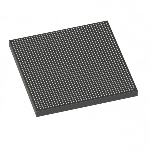
Overview of 5SGXEA5K1F40I2N – Stratix® V GX FPGA, 490,000 logic elements, ~46.08 Mbits embedded memory, 696 I/Os, 1517-BBGA
The 5SGXEA5K1F40I2N is a Stratix® V GX Field Programmable Gate Array (FPGA) IC designed for high-density, high-performance programmable logic applications. It combines a large logic fabric with substantial on-chip memory and a broad I/O complement in a 1517-BBGA FCBGA package for surface-mount assembly.
Targeted at industrial-grade applications, this device offers an industrial operating temperature range and a tight core voltage supply window, making it suitable for designs that require significant logic capacity, embedded memory, and extensive I/O connectivity.
Key Features
- Core Logic: 490,000 logic elements delivering substantial programmable logic resources for complex designs.
- Logic Array Blocks (CLBs): 185,000 CLBs for structured logic partitioning and implementation.
- Embedded Memory: Approximately 46.08 Mbits of on-chip RAM for buffering, packet buffering, and state storage within the fabric.
- I/O Density: 696 I/Os to support wide parallel interfaces and dense peripheral connectivity.
- Transceiver Capability (series-level): Stratix V GX family documentation includes multi-gigabit transceiver speed grades (series-level information in the device datasheet), enabling high-speed serial link implementations where applicable.
- Power and Voltage: Core supply specified at 870 mV to 930 mV for precise power delivery and core voltage management.
- Package and Mounting: 1517-BBGA (FCBGA) supplied in a 1517-FBGA (40×40) package footprint; surface-mount mounting type for standard PCB assembly.
- Industrial Grade & Temperature: Industrial temperature grade with an operating range of −40°C to 100°C for robust field deployment.
- Standards Compliance: RoHS compliant.
Typical Applications
- High-speed communications and networking: Large logic and on-chip memory combined with series-level multi-gigabit transceiver options support packet processing and high-throughput link implementations.
- Industrial and embedded systems: Industrial temperature grading and extensive I/O make this device suitable for industrial control, automation, and embedded processing tasks.
- Compute and acceleration fabrics: High logic element count and ample embedded RAM enable hardware acceleration and compute offload within custom platforms.
Unique Advantages
- Exceptional logic density: 490,000 logic elements provide the capacity to implement large, complex designs without immediate migration to multiple devices.
- Substantial embedded memory: Approximately 46.08 Mbits of on-chip RAM reduces the need for external memory in many buffering and state-storage scenarios.
- High I/O count: 696 I/Os facilitate wide parallel interfaces and dense connectivity for peripherals and mezzanine cards.
- Industrial readiness: Rated for −40°C to 100°C operation, supporting reliable deployment in harsher ambient conditions.
- Compact, manufacturable package: 1517-BBGA (FCBGA) surface-mount package balances high-pincount routing with industry-standard PCB assembly.
- Controlled core voltage: Narrow core supply range (870 mV–930 mV) enables consistent power design and predictable device behavior.
Why Choose 5SGXEA5K1F40I2N?
The 5SGXEA5K1F40I2N positions itself as a high-density Stratix V GX FPGA option for engineers who require substantial programmable logic, large on-chip memory, and extensive I/O in an industrial-grade package. Its combination of 490,000 logic elements, approximately 46.08 Mbits of embedded RAM, and 696 I/Os supports demanding implementations where integration and board-level simplicity are priorities.
Backed by the Stratix V device documentation for electrical and switching characteristics, this device is suited to development teams building industrial embedded platforms, high-speed communications equipment, and hardware-accelerated systems that need scalable logic capacity and reliable thermal performance.
Request a quote or submit an inquiry for pricing and availability to begin integration planning for the 5SGXEA5K1F40I2N.


Date Founded: 1968
Headquarters: Santa Clara, California, USA
Employees: 130,000+
Revenue: $54.23 Billion
Certifications and Memberships: ISO9001:2015, ISO14001:2015, ISO17025:2017, ISO27001:2022, ISO45001:2018, ISO50001:2018


