
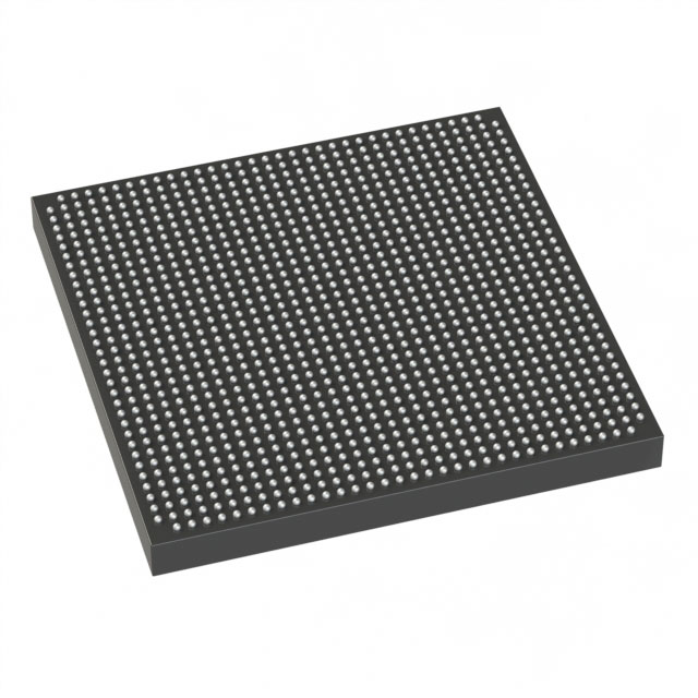
5SGXEA5K2F35C2G
| Part Description |
Stratix® V GX Field Programmable Gate Array (FPGA) IC 432 46080000 490000 1152-BBGA, FCBGA |
|---|---|
| Quantity | 151 Available (as of June 15, 2026) |
| Product Category | Field Programmable Gate Array (FPGA) |
|---|---|
| Manufacturer | Intel |
| Manufacturing Status | Active |
| Manufacturer Standard Lead Time | 26 Weeks |
| Datasheet |
Specifications & Environmental
| Device Package | 1152-FBGA (35x35) | Grade | Commercial | Operating Temperature | 0°C – 85°C | ||
|---|---|---|---|---|---|---|---|
| Package / Case | 1152-BBGA, FCBGA | Number of I/O | 432 | Voltage | 870 mV - 930 mV | ||
| Mounting Method | Surface Mount | RoHS Compliance | RoHS Compliant | REACH Compliance | REACH Unaffected | ||
| Moisture Sensitivity Level | 3 (168 Hours) | Number of LABs/CLBs | 185000 | Number of Logic Elements/Cells | 490000 | ||
| Number of Gates | N/A | ECCN | N/A | HTS Code | N/A | ||
| Qualification | N/A | Total RAM Bits | 46080000 |
Overview of 5SGXEA5K2F35C2G – Stratix® V GX FPGA, 490,000 logic elements, ~46 Mbits RAM, 432 I/Os, 1152‑BBGA
The 5SGXEA5K2F35C2G is an Intel Stratix® V GX field-programmable gate array (FPGA) device designed for high-density programmable logic and on-chip memory integration. This commercial-grade FPGA delivers approximately 490,000 logic elements, roughly 46 Mbits of embedded memory, and 432 I/O pins in a 1152‑BBGA (35×35 FCBGA) surface-mount package.
As part of the Stratix V GX family, the device is aligned with the series’ transceiver speed-grade offerings and device-level documentation. The device operates on a core voltage supply range of 870 mV to 930 mV and is specified for commercial temperature operation from 0 °C to 85 °C.
Key Features
- Core density Approximately 490,000 logic elements with 185,000 logic array blocks (LABs) to implement large-scale logic, datapaths, and custom accelerators.
- Embedded memory Approximately 46.08 Mbits of on-chip RAM for buffering, FIFOs, and memory-intensive logic functions.
- I/O and transceiver family support 432 user I/Os provided in the 1152‑BBGA package; Stratix V GX family documentation includes GX transceiver speed-grade options at the series level.
- Power and core voltage Core supply voltage specified between 870 mV and 930 mV to support regulated core operation.
- Package and mounting 1152‑BBGA, FCBGA package (supplier device package: 1152‑FBGA 35×35) optimized for surface-mount PCB assembly.
- Commercial grade and temperature range Commercial-grade device with operating temperature specified from 0 °C to 85 °C.
- Regulatory compliance RoHS compliant.
Typical Applications
- High-speed communications Leverage the Stratix V GX family’s transceiver speed-grade offerings together with dense logic and on-chip memory for protocol bridging and line-rate packet processing.
- Networking and switching High logic density and abundant I/O make the device suitable for custom switching, packet inspection, and hardware offload functions.
- Data acceleration Large embedded RAM and extensive logic resources support implementation of hardware accelerators and data-path optimizations.
Unique Advantages
- Significant logic capacity: The combination of ~490,000 logic elements and 185,000 LABs enables complex, high-density designs without partitioning across multiple devices.
- Substantial on-chip memory: Approximately 46 Mbits of embedded RAM reduces external memory dependence and improves data locality for high-throughput designs.
- Compact, production-ready package: 1152‑BBGA (35×35 FCBGA) surface-mount package provides a space-efficient solution for system integration.
- Predictable commercial operation: Specified core voltage range and 0 °C to 85 °C operating temperature simplify power budgeting and thermal planning for standard commercial deployments.
- RoHS compliant: Meets common environmental compliance requirements for modern electronic products.
Why Choose 5SGXEA5K2F35C2G?
The 5SGXEA5K2F35C2G positions itself as a high-density Stratix V GX FPGA option for designs that require extensive programmable logic, significant on-chip memory, and a large I/O footprint in a single commercial-grade package. Its specified core voltage range and operating temperature make it suitable for a broad range of commercial embedded, communications, and data-acceleration applications.
Engineers and system designers seeking a robust, well-documented Stratix V GX family device will find this part offers the capacity and integration necessary to consolidate functions, reduce board complexity, and support demanding logic and memory requirements.
Request a quote or submit an inquiry to receive current pricing and availability for the 5SGXEA5K2F35C2G.


Date Founded: 1968
Headquarters: Santa Clara, California, USA
Employees: 130,000+
Revenue: $54.23 Billion
Certifications and Memberships: ISO9001:2015, ISO14001:2015, ISO17025:2017, ISO27001:2022, ISO45001:2018, ISO50001:2018


