
5SGXEA5K2F35C2N
| Part Description |
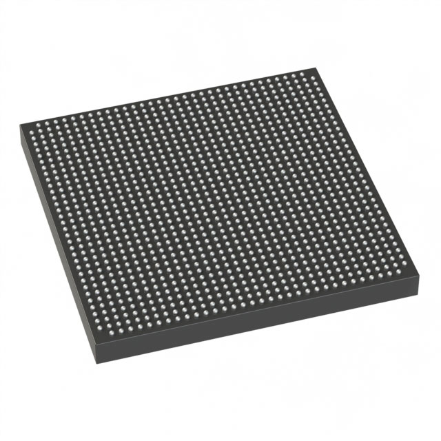
Stratix® V GX Field Programmable Gate Array (FPGA) IC 432 46080000 490000 1152-BBGA, FCBGA |
|---|---|
| Quantity | 654 Available (as of June 14, 2026) |

| Product Category | Field Programmable Gate Array (FPGA) |
|---|---|
| Manufacturer | Intel |
| Manufacturing Status | Obsolete |
| Manufacturer Standard Lead Time | Contact Us |
| Datasheet |
Specifications & Environmental
| Device Package | 1152-FBGA (35x35) | Grade | Commercial | Operating Temperature | 0°C – 85°C | ||
|---|---|---|---|---|---|---|---|
| Package / Case | 1152-BBGA, FCBGA | Number of I/O | 432 | Voltage | 870 mV - 930 mV | ||
| Mounting Method | Surface Mount | RoHS Compliance | RoHS Compliant | REACH Compliance | REACH Unknown | ||
| Moisture Sensitivity Level | 3 (168 Hours) | Number of LABs/CLBs | 185000 | Number of Logic Elements/Cells | 490000 | ||
| Number of Gates | N/A | ECCN | 3A001A2C | HTS Code | 8542.39.0001 | ||
| Qualification | N/A | Total RAM Bits | 46080000 |
Overview of 5SGXEA5K2F35C2N – Stratix® V GX FPGA, approximately 490,000 logic elements, ~46 Mbits RAM, 432 I/O, 1152‑FBGA
The 5SGXEA5K2F35C2N is an Intel Stratix® V GX Field Programmable Gate Array (FPGA) supplied in a 1152‑FBGA package. It delivers a high-density, commercial‑grade programmable fabric with substantial embedded memory and a large I/O count for complex digital designs.
With approximately 490,000 logic elements, roughly 46 Mbits of on‑chip RAM, and 432 user I/O, this device targets applications that require dense logic capacity, significant embedded memory, and extensive board-level interfacing while operating within commercial temperature limits.
Key Features
- Logic Capacity Approximately 490,000 logic elements suitable for large, multi‑functional FPGA designs.
- Embedded Memory Approximately 46 Mbits of on‑chip RAM for buffering, lookup tables, and state storage.
- I/O Density 432 user I/O pins to support wide parallel interfaces and multiple peripheral connections.
- Package and Mounting 1152‑BBGA / 1152‑FBGA package (35×35) in a surface‑mount format for board‑level integration.
- Supply Voltage Rated voltage supply range of 870 mV to 930 mV, enabling designs that target this core voltage window.
- Commercial Temperature Grade Specified operating temperature from 0 °C to 85 °C for commercial applications.
- RoHS Compliance Environmentally compliant (RoHS).
Typical Applications
- High‑density digital processing Large FPGA implementations that require substantial logic and embedded memory for algorithms, DSP, or packet processing.
- Multi‑interface systems Board designs that need many parallel or serial interfaces supported by a high I/O count.
- Prototyping and system integration Complex system prototypes and integration platforms that leverage reprogrammable logic and sizable on‑chip RAM.
Unique Advantages
- Substantial logic resources Approximately 490,000 logic elements reduce the need for external glue logic and enable more functionality in a single device.
- Large embedded memory Approximately 46 Mbits of on‑chip RAM supports deep buffering and localized data storage, lowering external memory dependence.
- High I/O count 432 I/O pins provide flexibility for complex interfacing and multiple simultaneous connections.
- Compact surface‑mount package 1152‑FBGA packaging delivers high density in a board‑mountable form factor for space‑constrained designs.
- Commercial temperature and RoHS compliant Designed for commercial environments with RoHS environmental compliance for broader market acceptance.
Why Choose 5SGXEA5K2F35C2N?
The 5SGXEA5K2F35C2N combines high logic density, considerable embedded memory, and a large I/O complement in a single commercial‑grade Stratix V GX FPGA. This device is suited for developers and system designers who must consolidate complex digital functions into one programmable device while maintaining a compact board footprint.
Its specification set—nearly half a million logic elements, roughly 46 Mbits of RAM, 432 I/O, and a 1152‑FBGA package—offers a clear path to reduce external components and simplify system architecture, with predictable operating conditions across the commercial temperature range.
Request a quote or submit a sales inquiry to evaluate 5SGXEA5K2F35C2N for your next high‑density FPGA design.


Date Founded: 1968
Headquarters: Santa Clara, California, USA
Employees: 130,000+
Revenue: $54.23 Billion
Certifications and Memberships: ISO9001:2015, ISO14001:2015, ISO17025:2017, ISO27001:2022, ISO45001:2018, ISO50001:2018


