
5SGXEA5N2F45C2L
| Part Description |
Stratix® V GX Field Programmable Gate Array (FPGA) IC 840 46080000 490000 1932-BBGA, FCBGA |
|---|---|
| Quantity | 1,009 Available (as of June 15, 2026) |

| Product Category | Field Programmable Gate Array (FPGA) |
|---|---|
| Manufacturer | Intel |
| Manufacturing Status | Obsolete |
| Manufacturer Standard Lead Time | Contact Us |
| Datasheet |
Specifications & Environmental
| Device Package | 1932-FBGA, FC (45x45) | Grade | Commercial | Operating Temperature | 0°C – 85°C | ||
|---|---|---|---|---|---|---|---|
| Package / Case | 1932-BBGA, FCBGA | Number of I/O | 840 | Voltage | 820 mV - 880 mV | ||
| Mounting Method | Surface Mount | RoHS Compliance | RoHS Compliant | REACH Compliance | REACH Unknown | ||
| Moisture Sensitivity Level | 3 (168 Hours) | Number of LABs/CLBs | 185000 | Number of Logic Elements/Cells | 490000 | ||
| Number of Gates | N/A | ECCN | 3A001A2C | HTS Code | 8542.39.0001 | ||
| Qualification | N/A | Total RAM Bits | 46080000 |
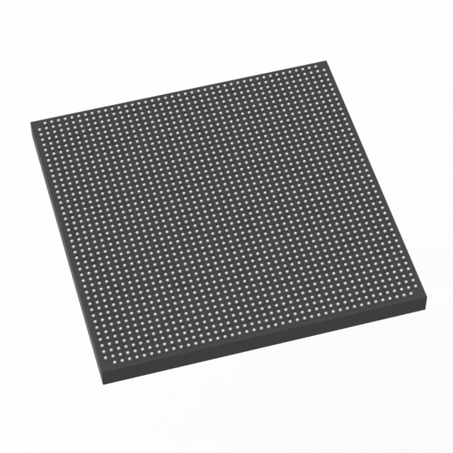
Overview of 5SGXEA5N2F45C2L – Stratix V GX FPGA, 490,000 logic elements, approximately 46 Mbit embedded memory, 840 I/Os
The 5SGXEA5N2F45C2L is a Stratix® V GX Field Programmable Gate Array (FPGA) IC offering high-density programmable logic for complex digital designs. This commercial-grade device integrates 490,000 logic elements and approximately 46 Mbits of on-chip RAM to support sizeable logic and memory requirements.
Packaged in a 1932-BBGA FCBGA (supplier package: 1932-FBGA, FC 45×45) with surface-mount assembly, the device provides up to 840 I/Os and operates from a core supply range of 820 mV to 880 mV within a commercial temperature range of 0 °C to 85 °C.
Key Features
- Core Logic 490,000 logic elements for implementing large-scale programmable logic and complex algorithms.
- Embedded Memory Approximately 46 Mbits of on-chip RAM to support buffering, state storage, and memory-intensive logic functions.
- I/O Density Up to 840 I/Os to interface with high-pin-count peripherals, parallel buses, and system I/O requirements.
- High-speed Transceiver Capability Stratix V GX family devices include GX transceiver channels with speed grades that can support up to 14.1 Gbps (speed-grade dependent), as documented in the Stratix V device datasheet.
- Power Core voltage supply range of 820 mV to 880 mV for compatibility with low-voltage FPGA power architectures.
- Package & Mounting 1932-BBGA, FCBGA package (supplier: 1932-FBGA, FC 45×45) optimized for surface-mount PCB assembly.
- Commercial Temperature Grade Rated for operation from 0 °C to 85 °C.
- Compliance RoHS compliant.
Typical Applications
- High-density digital processing Use the large logic capacity and embedded RAM to implement complex pipelines, custom accelerators, and parallel processing engines.
- High-speed interfaces and networking Leverage the GX transceiver family capability and 840 I/Os for data-paths, protocol bridging, and high-throughput link aggregation (transceiver speeds are speed-grade dependent).
- Telecommunications and datacom modules Combine high logic count and on-chip memory for packet processing, framing, and interface adaptation functions.
- System integration and prototyping The device’s high I/O count and dense logic make it suitable for consolidating multiple functions onto a single FPGA during system development and integration.
Unique Advantages
- High logic density: 490,000 logic elements enable implementation of large, complex designs without immediate migration to multi-device solutions.
- Significant embedded memory: Approximately 46 Mbits of on-chip RAM reduces dependence on external memory for many buffering and state-storage needs.
- Extensive I/O accessibility: Up to 840 I/Os support rich peripheral connectivity and parallel interfaces, simplifying board-level design.
- Family-level transceiver capability: Stratix V GX devices document GX channels with multi-gigabit capability (up to 14.1 Gbps, speed-grade dependent), enabling high-bandwidth links where required.
- Compact, industry-standard packaging: 1932-BBGA (45×45 mm supplier footprint) provides a high-pin-count solution in a surface-mount form factor.
- Regulatory and assembly readiness: RoHS compliance and standard surface-mount packaging support modern manufacturing and environmental requirements.
Why Choose 5SGXEA5N2F45C2L?
The 5SGXEA5N2F45C2L positions itself as a high-density Stratix V GX FPGA option for designs that require substantial programmable logic, sizeable on-chip memory, and a large number of I/Os. Its package and power envelope suit complex board-level integrations where a single FPGA can consolidate multiple subsystems.
Engineers and procurement teams targeting commercial-temperature applications will find the device’s combination of logic resources, embedded memory, and documented Stratix V GX transceiver capabilities useful for scalable designs that may evolve across speed-grade and feature requirements within the Stratix V family.
Request a quote or submit a brief inquiry to begin evaluating the 5SGXEA5N2F45C2L for your next design and to obtain pricing and availability information.


Date Founded: 1968
Headquarters: Santa Clara, California, USA
Employees: 130,000+
Revenue: $54.23 Billion
Certifications and Memberships: ISO9001:2015, ISO14001:2015, ISO17025:2017, ISO27001:2022, ISO45001:2018, ISO50001:2018


