
5SGXEA7K2F40I2N
| Part Description |
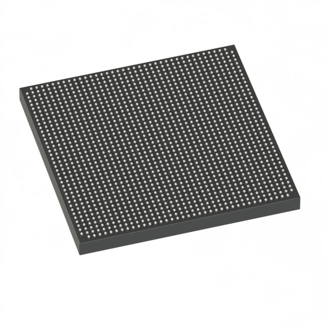
Stratix® V GX Field Programmable Gate Array (FPGA) IC 696 51200000 622000 1517-BBGA, FCBGA |
|---|---|
| Quantity | 1,729 Available (as of June 15, 2026) |

| Product Category | Field Programmable Gate Array (FPGA) |
|---|---|
| Manufacturer | Intel |
| Manufacturing Status | Obsolete |
| Manufacturer Standard Lead Time | Contact Us |
| Datasheet |
Specifications & Environmental
| Device Package | 1517-FBGA (40x40) | Grade | Industrial | Operating Temperature | -40°C – 100°C | ||
|---|---|---|---|---|---|---|---|
| Package / Case | 1517-BBGA, FCBGA | Number of I/O | 696 | Voltage | 870 mV - 930 mV | ||
| Mounting Method | Surface Mount | RoHS Compliance | RoHS Compliant | REACH Compliance | REACH Unknown | ||
| Moisture Sensitivity Level | 3 (168 Hours) | Number of LABs/CLBs | 234720 | Number of Logic Elements/Cells | 622000 | ||
| Number of Gates | N/A | ECCN | 3A001A2C | HTS Code | 8542.39.0001 | ||
| Qualification | N/A | Total RAM Bits | 51200000 |
Overview of 5SGXEA7K2F40I2N – Stratix® V GX FPGA, 696 I/Os, approximately 51.2 Mbit RAM
The 5SGXEA7K2F40I2N is an Intel Stratix® V GX Field Programmable Gate Array (FPGA) supplied in a 1517-BBGA FCBGA package. It delivers high logic and I/O capacity—622,000 logic elements and 696 I/Os—along with approximately 51.2 Mbits of embedded memory for demanding programmable-logic applications.
Designed for industrial-grade environments, this device supports a core supply voltage range of 870 mV to 930 mV and an operating temperature range from -40 °C to 100 °C, making it suitable for robust, high-density designs that require large on-chip resources and wide I/O counts.
Key Features
- Core Capacity Provides 622,000 logic elements, enabling implementation of complex custom logic and large-scale compute fabrics.
- Logic Array Blocks Includes 234,720 logic array blocks for structured resource partitioning and design scalability.
- Embedded Memory Approximately 51.2 Mbits of on-chip RAM to support buffering, large FIFOs, and memory-intensive algorithms without external memory dependence.
- I/O Resources 696 differential and single‑ended I/Os to support wide parallel interfaces, multi-protocol connectivity, and high pin-count system integration.
- Package 1517-BBGA (FCBGA) supplier device package 1517-FBGA (40×40) for dense board-level integration and reliable solder mounting.
- Power Core voltage supply specified between 870 mV and 930 mV to enable consistent power budgeting and design margining.
- Thermal & Grade Industrial temperature grade with an operating range of -40 °C to 100 °C for extended-environment deployments.
- Mounting Surface-mount package compatible with standard board-assembly processes.
- Compliance RoHS compliant to meet standard environmental and manufacturing requirements.
Typical Applications
- High-density digital signal processing Use the large logic element count and substantial embedded memory to implement complex DSP pipelines and large parallel processing blocks.
- Custom hardware acceleration Leverage the high logic capacity and abundant I/Os for FPGA-based accelerators and offload engines in compute systems.
- Interface bridging and protocol translation The extended I/O count supports multi-protocol gateway designs and high-pin-count peripheral interfacing.
Unique Advantages
- High logic density: 622,000 logic elements provide the headroom to implement large, integrated designs without immediate need for multiple FPGAs.
- Large on‑chip memory: Approximately 51.2 Mbits of embedded RAM reduces external memory dependency and simplifies board-level BOM and routing.
- Extensive I/O capacity: 696 I/Os enable broad connectivity for multi-lane interfaces, multiple peripherals, and wide parallel buses.
- Industrial-ready thermal range: Rated for -40 °C to 100 °C operation to support deployments in harsh or temperature-variable environments.
- Compact, high-density package: 1517-BBGA FCBGA (supplier 1517-FBGA 40×40) balances pin count and board area for dense system integration.
- Regulatory readiness: RoHS compliance simplifies environmental qualification in end products.
Why Choose 5SGXEA7K2F40I2N?
The 5SGXEA7K2F40I2N combines very large logic capacity, substantial embedded memory, and an expansive I/O complement in an industrial-grade Stratix V GX FPGA package. Its electrical and thermal specifications support robust system designs that demand on-chip resources and wide interfacing capability.
This device is ideal for engineering teams building complex, high-density programmable logic systems where integration, scalability, and environmental robustness are required. Its combination of resources helps reduce external components and supports long-term design scalability within the Stratix V family specification framework.
Request a quote or submit an inquiry to receive pricing, availability, and lead-time information for the 5SGXEA7K2F40I2N.


Date Founded: 1968
Headquarters: Santa Clara, California, USA
Employees: 130,000+
Revenue: $54.23 Billion
Certifications and Memberships: ISO9001:2015, ISO14001:2015, ISO17025:2017, ISO27001:2022, ISO45001:2018, ISO50001:2018


