
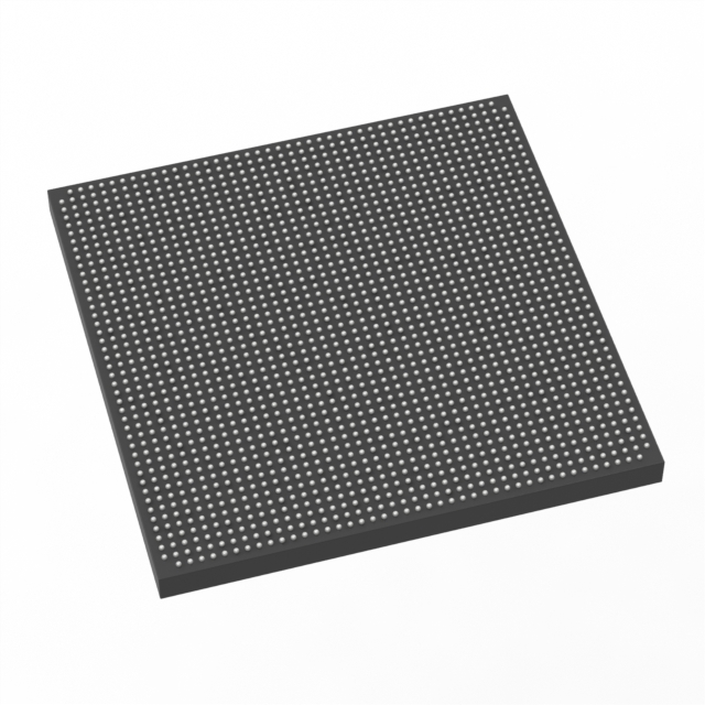
5SGXEA7N2F45C2LN
| Part Description |
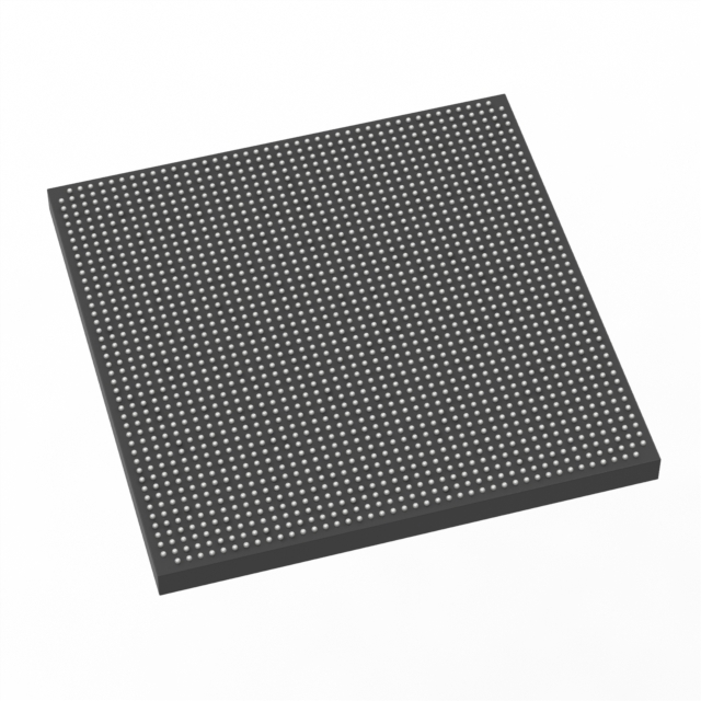
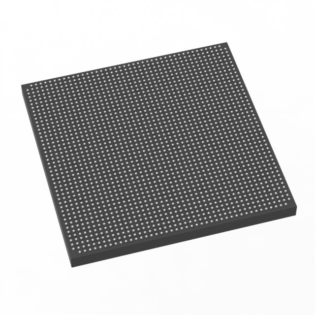
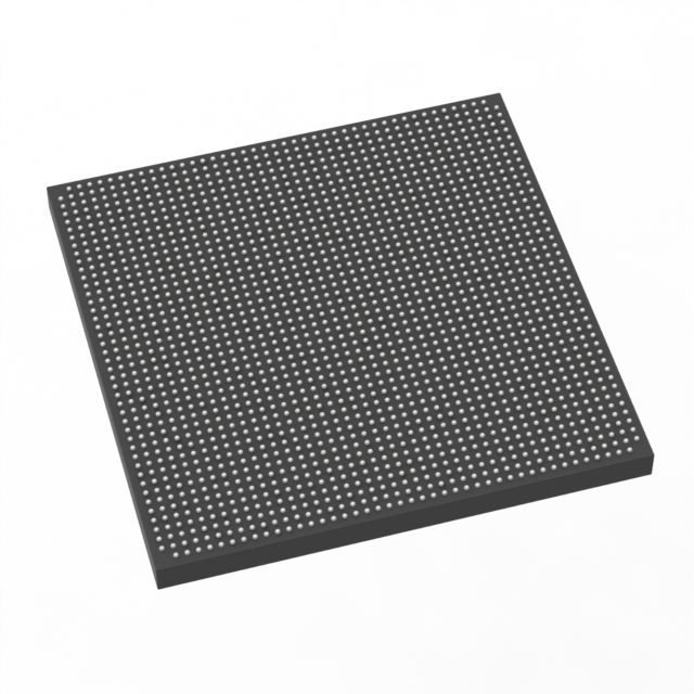
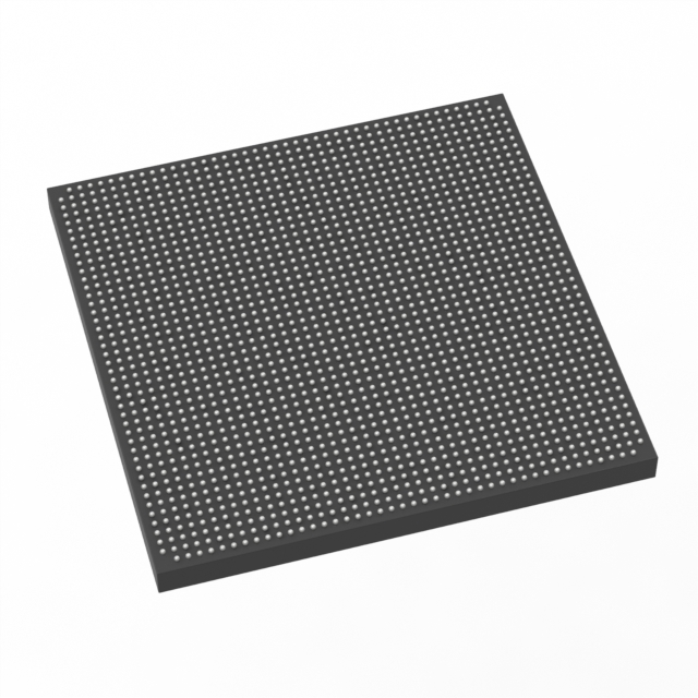
Stratix® V GX Field Programmable Gate Array (FPGA) IC 840 51200000 622000 1932-BBGA, FCBGA |
|---|---|
| Quantity | 349 Available (as of October 7, 2026) |
| Product Category | Field Programmable Gate Array (FPGA) |
|---|---|
| Manufacturer | Intel |
| Manufacturing Status | Obsolete |
| Manufacturer Standard Lead Time | Contact Us |
| Datasheet |
Specifications & Environmental
| Device Package | 1932-FBGA, FC (45x45) | Grade | Commercial | Operating Temperature | 0°C – 85°C | ||
|---|---|---|---|---|---|---|---|
| Package / Case | 1932-BBGA, FCBGA | Number of I/O | 840 | Voltage | 820 mV - 880 mV | ||
| Mounting Method | Surface Mount | RoHS Compliance | RoHS Compliant | REACH Compliance | REACH Unknown | ||
| Moisture Sensitivity Level | 3 (168 Hours) | Number of LABs/CLBs | 234720 | Number of Logic Elements/Cells | 622000 | ||
| Number of Gates | N/A | ECCN | 3A001A2C | HTS Code | 8542.39.0001 | ||
| Qualification | N/A | Total RAM Bits | 51200000 |
Overview of 5SGXEA7N2F45C2LN – Stratix® V GX Field Programmable Gate Array (FPGA) IC, 840 I/O, approximately 51.2 Mbits RAM, 622,000 logic elements, 1932-BBGA
The 5SGXEA7N2F45C2LN is a commercial-grade Stratix V GX family FPGA that delivers high logic density and large embedded memory in a single surface-mount FCBGA package. Designed for applications that demand substantial on-chip logic, extensive I/O, and significant embedded RAM, this device integrates core fabric and family-level transceiver capabilities described in the Stratix V GX datasheet.
This device targets designs requiring a compact, high-density programmable platform with clearly defined supply and thermal envelopes for mainstream commercial products.
Key Features
- Core Logic Capacity 622,000 logic elements and 234,720 logic blocks provide substantial programmable logic resources for complex designs.
- Embedded Memory Approximately 51.2 Mbits of on-chip RAM to support large buffering, lookup tables, and intermediate data storage.
- I/O Count 840 I/O pins enable wide parallel interfaces and extensive connectivity for peripherals and external devices.
- Power Supply Specified core voltage supply range of 820 mV to 880 mV for defined power and timing behavior in the target operating window.
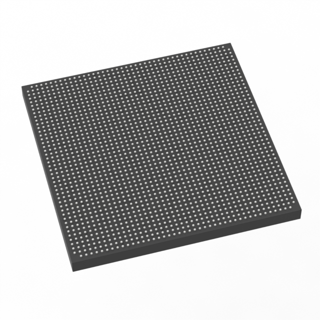
- Package & Mounting 1932-BBGA FCBGA package (supplier package: 1932-FBGA, FC, 45×45) in a surface-mount form factor for high-density board integration.
- Grade & Temperature Commercial grade with an operating temperature range of 0 °C to 85 °C suitable for mainstream commercial electronic products.
- RoHS Compliance RoHS-compliant to meet common environmental and manufacturing requirements.
- Series-Level Transceiver Capability (datasheet) The Stratix V GX family documentation describes transceiver speed grades up to 14.1 Gbps, providing high-speed serial interface options at the family level.
Typical Applications
- High-density logic systems Use the device where large programmable logic capacity is required for complex state machines, custom accelerators, or FPGA-based processing pipelines.
- Memory-intensive buffering On-chip RAM (~51.2 Mbits) supports large FIFOs, packet buffers, and data staging for high-throughput designs.
- I/O-rich control and interface hubs The 840 I/O pins enable broad parallel connectivity for interface aggregation, sensor arrays, and multi-channel data capture.
- High-speed serial systems (family-level) Leverage the Stratix V GX family transceiver capability described in the datasheet for designs that require high-bandwidth serial links.
Unique Advantages
- Substantial logic and memory in one device: The combination of 622,000 logic elements and approximately 51.2 Mbits of embedded RAM reduces the need for external logic and memory, simplifying system architecture.
- High I/O count for complex interfacing: 840 I/Os let you consolidate multiple interfaces and parallel channels on a single FPGA, reducing board complexity and connector count.
- Commercial-grade thermal profile: Rated for 0 °C to 85 °C to match mainstream commercial product requirements while keeping thermal design straightforward.
- Defined power envelope: Core supply range of 820 mV–880 mV supports predictable power and timing characteristics within the specified operating window.
- Compact, high-density package: The 1932-BBGA (FCBGA) 45×45 supplier package enables high-density PCB layouts for space-constrained applications.
- RoHS-compliant manufacturing: Environmentally compliant component choice for contemporary product assemblies.
Why Choose 5SGXEA7N2F45C2LN?
The 5SGXEA7N2F45C2LN brings large-scale programmable logic, substantial on-chip memory, and a high I/O count together in a single commercial-grade FCBGA package. Its clear power and thermal specifications make it suitable for mainstream commercial deployments that require significant integration without splitting functions across multiple discrete devices.
Engineers and procurement teams will find this FPGA appropriate for designs that demand high-density logic resources, extensive buffering, and broad peripheral connectivity, while remaining within a well-defined commercial operating envelope and RoHS compliance.
Request a quote or submit an inquiry to receive pricing, availability, and further technical information for 5SGXEA7N2F45C2LN.





















Date Founded: 1968
Headquarters: Santa Clara, California, USA
Employees: 130,000+
Revenue: $54.23 Billion
Certifications and Memberships: ISO9001:2015, ISO14001:2015, ISO17025:2017, ISO27001:2022, ISO45001:2018, ISO50001:2018


