
5SGXEA9K3H40I3LN
| Part Description |
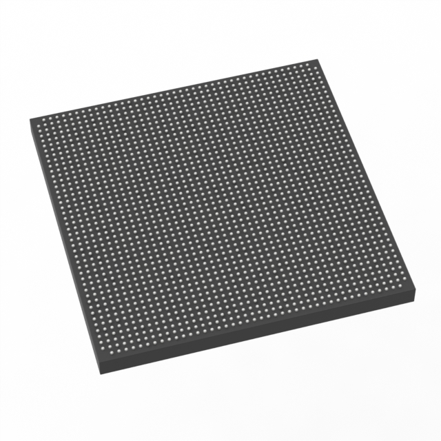
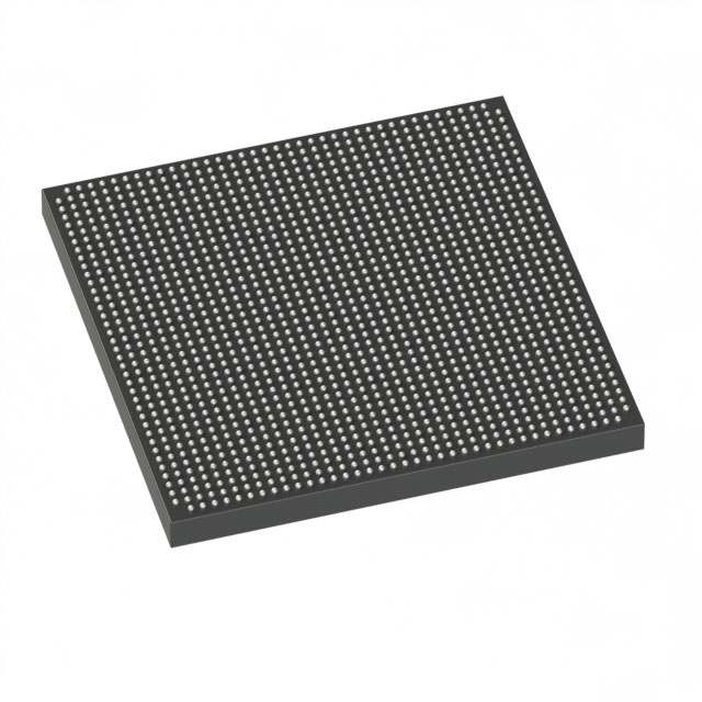
Stratix® V GX Field Programmable Gate Array (FPGA) IC 696 53248000 840000 1517-BBGA, FCBGA |
|---|---|
| Quantity | 436 Available (as of June 15, 2026) |

| Product Category | Field Programmable Gate Array (FPGA) |
|---|---|
| Manufacturer | Intel |
| Manufacturing Status | Obsolete |
| Manufacturer Standard Lead Time | Contact Us |
| Datasheet |
Specifications & Environmental
| Device Package | 1517-HBGA (45x45) | Grade | Industrial | Operating Temperature | -40°C – 100°C | ||
|---|---|---|---|---|---|---|---|
| Package / Case | 1517-BBGA, FCBGA | Number of I/O | 696 | Voltage | 820 mV - 880 mV | ||
| Mounting Method | Surface Mount | RoHS Compliance | RoHS Compliant | REACH Compliance | REACH Unknown | ||
| Moisture Sensitivity Level | 3 (168 Hours) | Number of LABs/CLBs | 317000 | Number of Logic Elements/Cells | 840000 | ||
| Number of Gates | N/A | ECCN | 3A001A2C | HTS Code | 8542.39.0001 | ||
| Qualification | N/A | Total RAM Bits | 53248000 |
Overview of 5SGXEA9K3H40I3LN – Stratix® V GX Field Programmable Gate Array (FPGA), 1517-BBGA FCBGA
The 5SGXEA9K3H40I3LN is a Stratix V GX family FPGA IC designed for industrial-grade, high-capacity programmable logic implementations. It combines a very large logic fabric with substantial on‑chip memory and extensive I/O density to address complex, I/O‑intensive designs.
Key value propositions include a large logic element count, approximately 53 Mbits of embedded memory, hundreds of user I/Os, and an industrial operating temperature range—making it suitable for demanding embedded and infrastructure applications that require significant programmable logic and memory resources.
Key Features
- Logic Capacity Provides 840,000 logic elements for implementing large-scale digital designs and complex logic functions.
- Embedded Memory Includes a total of 53,248,000 bits of on-chip RAM (approximately 53 Mbits) to support buffering, tables, and local data storage.
- I/O Density Offers 696 user I/O pins to support a wide range of external interfaces and high-channel-count connections.
- Package Supplied in a 1517‑BBGA FCBGA package (supplier device package: 1517‑HBGA, 45×45), optimized for high pin-count surface-mount deployment.
- Power Core voltage supply range of 820 mV to 880 mV to match required FPGA core power rails.
- Industrial Temperature Grade Specified for operation from −40 °C to 100 °C for industrial-environment reliability.
- Mounting Surface mount package suitable for PCB assembly processes.
- Regulatory RoHS compliant for lead‑free manufacturing and environmental requirements.
Typical Applications
- High-density networking and switching Large logic capacity and high I/O count enable packet processing and protocol handling in infrastructure equipment.
- Signal processing and compute acceleration Substantial logic elements and embedded RAM support real-time DSP, compute offload, and data-path implementations.
- Industrial control and automation Industrial temperature rating and robust I/O make the device suited for control systems and automation platforms requiring on-board programmability.
- Custom system integration High I/O density and a large programmable fabric allow integration of multiple functions into a single FPGA for space- and BOM-constrained designs.
Unique Advantages
- Large on-chip logic and memory: 840,000 logic elements combined with approximately 53 Mbits of embedded RAM reduce the need for external logic and memory components.
- High I/O availability: 696 user I/Os support dense connectivity and multiple parallel interfaces without additional multiplexing hardware.
- Industrial temperature rating: Rated from −40 °C to 100 °C for reliable operation in harsher environments and extended temperature ranges.
- Compact high-pin-count package: 1517‑BBGA / 1517‑HBGA (45×45) package delivers high pin density in a surface-mount form factor for advanced board layouts.
- Defined low-voltage core: 820–880 mV supply requirement aligns with modern low-voltage FPGA cores for power-managed system designs.
- RoHS compliant: Supports lead‑free manufacturing workflows and environmental compliance needs.
Why Choose 5SGXEA9K3H40I3LN?
The 5SGXEA9K3H40I3LN positions itself as a high-capacity, industrial-grade Stratix V GX FPGA suitable for designs that demand significant programmable logic, on-chip memory, and extensive I/O. Its combination of 840,000 logic elements, approximately 53 Mbits of embedded RAM, and nearly 700 I/Os supports consolidation of complex subsystems into a single device, simplifying BOM and board-level complexity.
This device is appropriate for engineering teams developing infrastructure, signal processing, or industrial control systems that require a robust, high-density programmable platform with industrial temperature support and a high-pin-count package for advanced integrations.
Request a quote or submit a procurement inquiry to learn about availability, pricing, and lead times for the 5SGXEA9K3H40I3LN.


Date Founded: 1968
Headquarters: Santa Clara, California, USA
Employees: 130,000+
Revenue: $54.23 Billion
Certifications and Memberships: ISO9001:2015, ISO14001:2015, ISO17025:2017, ISO27001:2022, ISO45001:2018, ISO50001:2018


