
5SGXEA9N1F45C2LN
| Part Description |
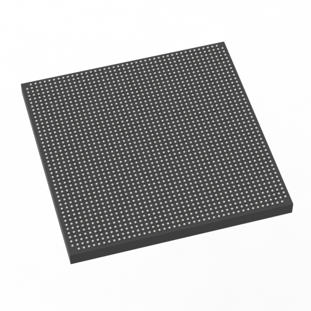
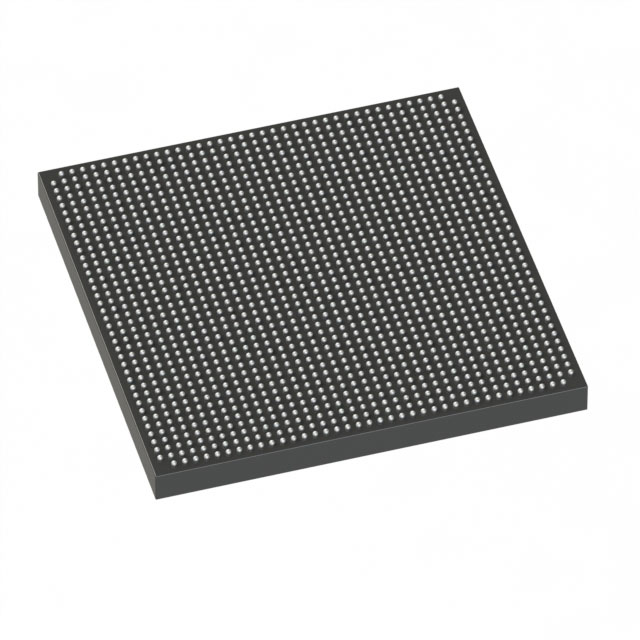
Stratix® V GX Field Programmable Gate Array (FPGA) IC 840 53248000 840000 1932-BBGA, FCBGA |
|---|---|
| Quantity | 1,324 Available (as of June 16, 2026) |
| Product Category | Field Programmable Gate Array (FPGA) |
|---|---|
| Manufacturer | Intel |
| Manufacturing Status | Obsolete |
| Manufacturer Standard Lead Time | Contact Us |
| Datasheet |
Specifications & Environmental
| Device Package | 1932-FBGA, FC (45x45) | Grade | Commercial | Operating Temperature | 0°C – 85°C | ||
|---|---|---|---|---|---|---|---|
| Package / Case | 1932-BBGA, FCBGA | Number of I/O | 840 | Voltage | 820 mV - 880 mV | ||
| Mounting Method | Surface Mount | RoHS Compliance | RoHS Compliant | REACH Compliance | REACH Unknown | ||
| Moisture Sensitivity Level | 3 (168 Hours) | Number of LABs/CLBs | 317000 | Number of Logic Elements/Cells | 840000 | ||
| Number of Gates | N/A | ECCN | 3A001A2C | HTS Code | 8542.39.0001 | ||
| Qualification | N/A | Total RAM Bits | 53248000 |
Overview of 5SGXEA9N1F45C2LN – Stratix V GX FPGA, 840,000 Logic Elements, 1932‑BBGA
The 5SGXEA9N1F45C2LN is a Stratix® V GX Field Programmable Gate Array (FPGA) in a 1932‑ball BGA package intended for commercial temperature applications. The device provides very high logic density and extensive on‑chip RAM and I/O resources for complex, programmable digital designs.
With 840,000 logic elements, approximately 53.25 Mbits of embedded memory and 840 user I/O pins, this FPGA targets designs that require large-scale programmable logic, ample embedded memory, and dense I/O integration while operating within a commercial temperature range.
Key Features
- Core Logic 840,000 logic elements (cells) to implement large, parallelizable digital designs and complex state machines.
- Embedded Memory Approximately 53.25 Mbits of on‑chip RAM available for buffering, FIFOs, and memory‑intensive functions.
- I/O Capacity 840 user I/O pins to support high‑pin‑count interfaces, dense board routing, and multi‑channel connectivity.
- Power Supply Core supply range specified at 820 mV to 880 mV to align with system power‑rail planning and decoupling requirements.
- Package & Mounting 1932‑BBGA (FCBGA) supplier package (1932‑FBGA, FC 45×45) in a surface‑mount form factor for compact, high‑density PCB layouts.
- Temperature & Grade Commercial grade with an operating temperature range of 0 °C to 85 °C, specified for standard commercial environments.
- Compliance RoHS compliant, supporting environmental and regulatory sourcing requirements.
Typical Applications
- High‑performance digital signal processing Use the device’s 840,000 logic elements and large embedded RAM to implement wide parallel datapaths and multi‑channel DSP algorithms.
- Networking and packet processing Large logic capacity and 840 I/O pins enable implementation of custom packet engines, switching logic, and high‑density interface aggregation.
- Compute acceleration and prototyping High logic density and significant on‑chip memory make the device suitable for hardware acceleration and system prototyping where programmable hardware resources are required.
Unique Advantages
- High logic density: 840,000 logic elements let you consolidate complex functions into a single device, reducing multi‑device BOM and board complexity.
- Substantial embedded memory: Approximately 53.25 Mbits of RAM supports large buffers, FIFOs, and memory‑centric functions without external memory for many use cases.
- Extensive I/O availability: 840 I/O pins provide flexibility for interfacing to multiple peripherals, buses, and high‑channel counts on a single FPGA.
- Compact, high‑density package: The 1932‑BBGA FCBGA package enables dense PCB integration while keeping the device footprint manageable for complex boards.
- Commercial temperature suitability: Rated for 0 °C to 85 °C operation, aligning with a wide range of standard commercial electronics deployments.
- RoHS compliant: Meets environmental sourcing expectations for many global supply chains.
Why Choose 5SGXEA9N1F45C2LN?
The 5SGXEA9N1F45C2LN combines very high logic capacity, significant embedded RAM and a large I/O count in a single commercial‑grade Stratix V GX FPGA package. It is well suited to designers who need to implement complex, memory‑intensive and I/O‑rich programmable logic on a compact board footprint while maintaining compliance with RoHS requirements.
This device is positioned for engineering teams developing high‑density FPGA designs that require a balance of logic resources, on‑chip memory and pin‑out flexibility, backed by Stratix V family documentation and support materials.
Request a quote or submit an inquiry to check availability, pricing, and lead time for the 5SGXEA9N1F45C2LN. Our team can provide a formal quote and assist with sourcing for your project.


Date Founded: 1968
Headquarters: Santa Clara, California, USA
Employees: 130,000+
Revenue: $54.23 Billion
Certifications and Memberships: ISO9001:2015, ISO14001:2015, ISO17025:2017, ISO27001:2022, ISO45001:2018, ISO50001:2018


