
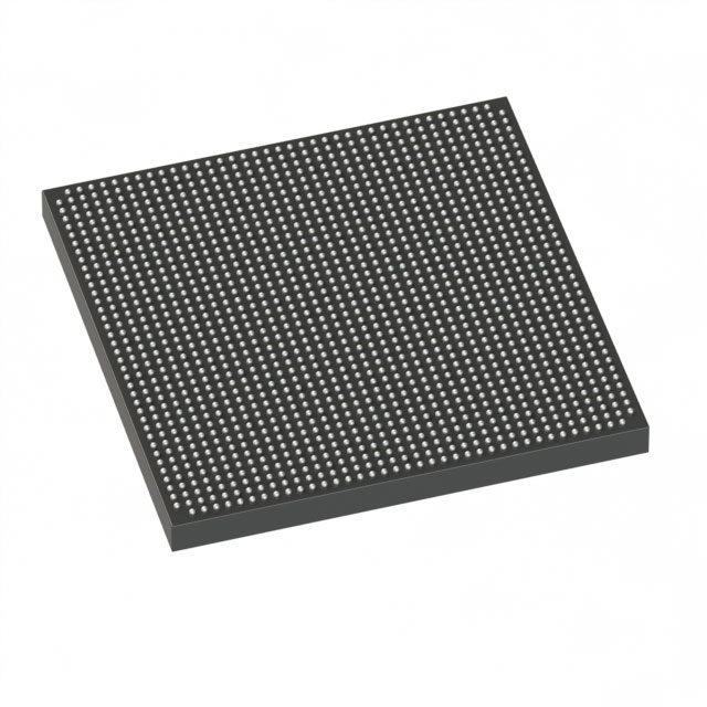
5SGXEB5R2F40C2L
| Part Description |
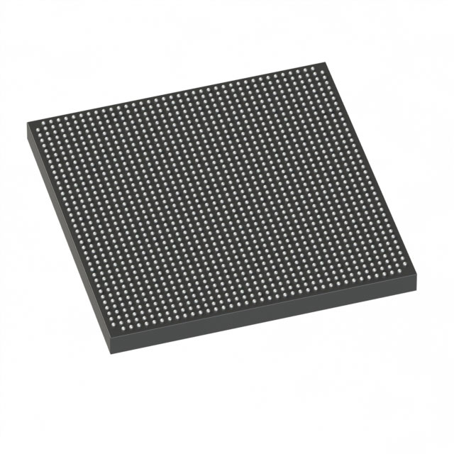
Stratix® V GX Field Programmable Gate Array (FPGA) IC 432 41984000 490000 1517-FBGA (40x40) |
|---|---|
| Quantity | 1,281 Available (as of October 8, 2026) |
| Product Category | Field Programmable Gate Array (FPGA) |
|---|---|
| Manufacturer | Intel |
| Manufacturing Status | Obsolete |
| Manufacturer Standard Lead Time | Contact Us |
| Datasheet |
Specifications & Environmental
| Device Package | 1517-FBGA (40x40) | Grade | Commercial | Operating Temperature | 0°C – 85°C | ||
|---|---|---|---|---|---|---|---|
| Package / Case | 1517-FBGA (40x40) | Number of I/O | 432 | Voltage | 820 mV - 880 mV | ||
| Mounting Method | Surface Mount | RoHS Compliance | RoHS Compliant | REACH Compliance | REACH Unknown | ||
| Moisture Sensitivity Level | 3 (168 Hours) | Number of LABs/CLBs | 185000 | Number of Logic Elements/Cells | 490000 | ||
| Number of Gates | N/A | ECCN | 3A001A2C | HTS Code | 8542.39.0001 | ||
| Qualification | N/A | Total RAM Bits | 41984000 |
Overview of 5SGXEB5R2F40C2L – Stratix® V GX FPGA IC, 490,000 logic elements, 432 I/Os, 1517‑FBGA
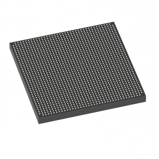
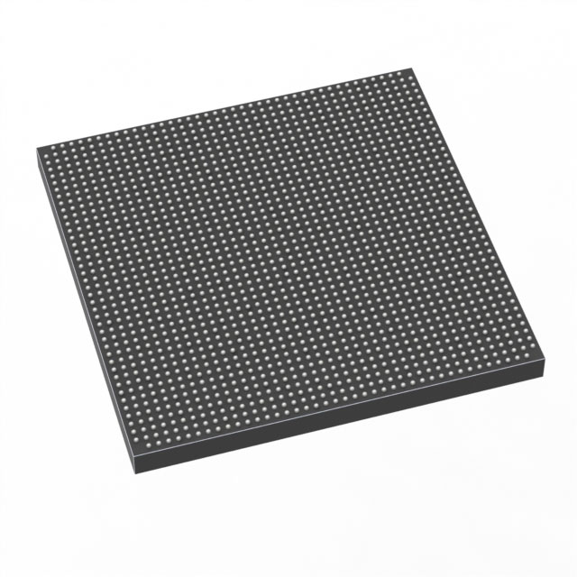
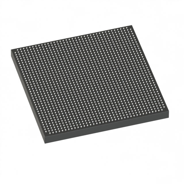
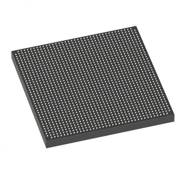
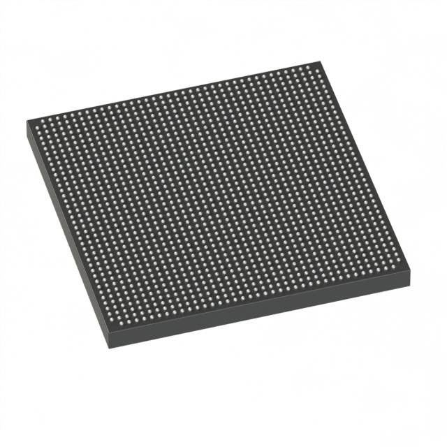
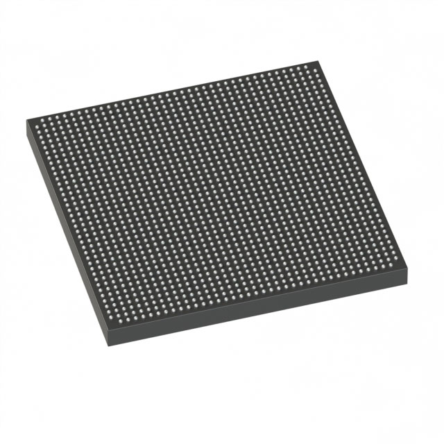
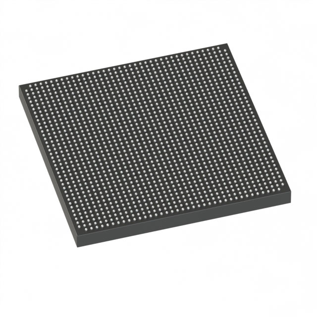
The 5SGXEB5R2F40C2L is a Stratix® V GX field‑programmable gate array (FPGA) offered in a 1517‑FBGA (40×40) package. It delivers a high on‑chip resource count and expansive I/O capability for complex, reconfigurable digital designs in commercial temperature environments.
Engineered for applications that require large logic capacity and significant embedded memory, this device balances dense logic resources, substantial RAM, and a broad I/O count while operating within a core supply range of 820 mV to 880 mV.
Key Features
- Logic Capacity Approximately 490,000 logic elements and 185,000 logic blocks provide abundant programmable fabric for large-scale designs.
- Embedded Memory Total on‑chip RAM of 41,984,000 bits (approximately 40 Mbits) supports deep buffering and on‑chip data structures for high‑throughput processing.
- I/O Density 432 I/Os enable extensive external interfacing for multi‑channel designs, peripherals, and high‑pin‑count system topologies.
- Power and Core Supply Core voltage supply specified from 820 mV to 880 mV to support the device’s operating requirements.
- Package & Mounting 1517‑FBGA (40×40) package in a surface‑mount form factor for compact board integration.
- Commercial Temperature Grade Specified operating temperature range of 0°C to 85°C for commercial applications.
- RoHS Compliant Manufactured in compliance with RoHS environmental standards.
Typical Applications
- High‑Density Signal Processing Use the large logic element count and on‑chip RAM to implement parallel DSP pipelines, filtering, and protocol processing.
- Multi‑Channel Interface Hubs 432 I/Os support aggregation and bridging of numerous peripherals, sensors, or data lanes in communication and instrumentation products.
- Reconfigurable Prototyping and Acceleration Leverage the extensive programmable fabric for hardware acceleration, algorithm prototyping, and system validation in commercial designs.
Unique Advantages
- Substantial Logic Resources: The combination of ~490,000 logic elements and 185,000 logic blocks lets designers implement complex state machines, datapaths, and custom ISAs on a single device.
- Large Embedded Memory: Nearly 42 million bits of on‑chip RAM reduce external memory dependence and improve determinism for buffering and local storage.
- High I/O Count: 432 I/Os simplify board‑level routing for multi‑lane interfaces and dense connector requirements, reducing the need for additional I/O expanders.
- Compact, Surface‑Mount Package: The 1517‑FBGA (40×40) package enables compact PCB layouts while maintaining high pin density for complex systems.
- Commercial‑Grade Operating Range: Specified 0°C to 85°C operation aligns with commercial product requirements and development workflows.
- Standards‑Aware Manufacture: RoHS compliance supports environmental and regulatory requirements for commercial electronics.
Why Choose 5SGXEB5R2F40C2L?
The 5SGXEB5R2F40C2L positions itself as a high‑capacity, commercially graded FPGA option when significant logic density, embedded RAM, and large I/O counts are primary design drivers. Its resource mix is well suited to teams developing data‑intensive, reconfigurable systems that require substantial on‑chip memory and numerous external interfaces.
For design teams seeking scalability within the Stratix V family and wanting a compact FBGA package with surface‑mount convenience, this device provides a balanced platform for prototyping and commercial deployment with documented operating and electrical characteristics.
Request a quote or submit an inquiry to receive availability, pricing, and ordering information for 5SGXEB5R2F40C2L. Our team can assist with lead times and procurement details tailored to your project schedule.





















Date Founded: 1968
Headquarters: Santa Clara, California, USA
Employees: 130,000+
Revenue: $54.23 Billion
Certifications and Memberships: ISO9001:2015, ISO14001:2015, ISO17025:2017, ISO27001:2022, ISO45001:2018, ISO50001:2018


