
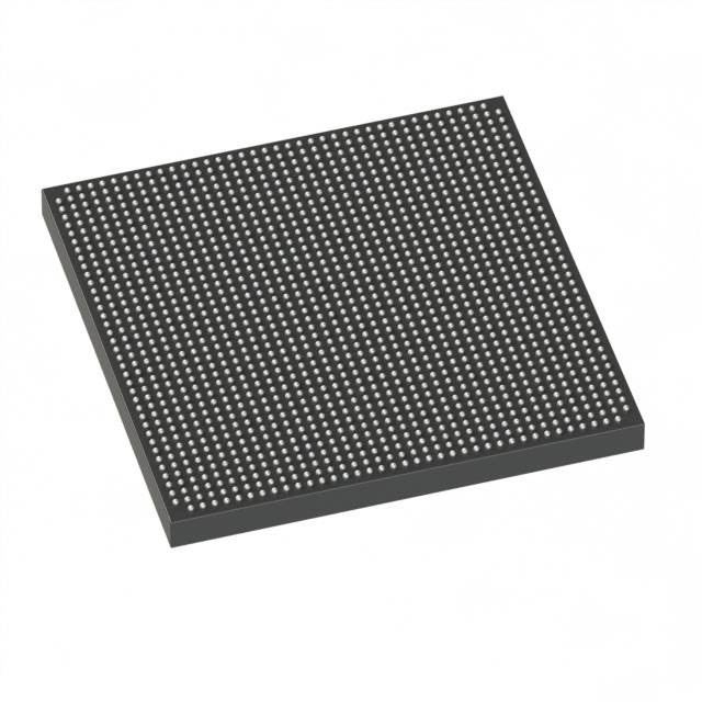
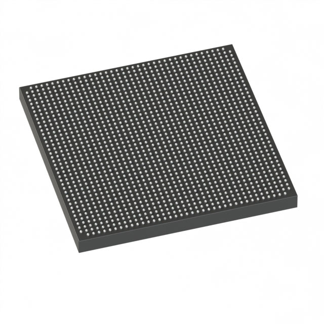
5SGXEB5R2F40C1G
| Part Description |
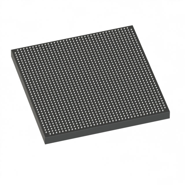
Stratix® V GX Field Programmable Gate Array (FPGA) IC 432 41984000 490000 1517-FBGA (40x40) |
|---|---|
| Quantity | 440 Available (as of October 8, 2026) |
| Product Category | Field Programmable Gate Array (FPGA) |
|---|---|
| Manufacturer | Intel |
| Manufacturing Status | Active |
| Manufacturer Standard Lead Time | 26 Weeks |
| Datasheet |
Specifications & Environmental
| Device Package | 1517-FBGA (40x40) | Grade | Commercial | Operating Temperature | 0°C – 85°C | ||
|---|---|---|---|---|---|---|---|
| Package / Case | 1517-FBGA (40x40) | Number of I/O | 432 | Voltage | 870 mV - 930 mV | ||
| Mounting Method | Surface Mount | RoHS Compliance | RoHS Compliant | REACH Compliance | REACH Unaffected | ||
| Moisture Sensitivity Level | 3 (168 Hours) | Number of LABs/CLBs | 185000 | Number of Logic Elements/Cells | 490000 | ||
| Number of Gates | N/A | ECCN | N/A | HTS Code | N/A | ||
| Qualification | N/A | Total RAM Bits | 41984000 |
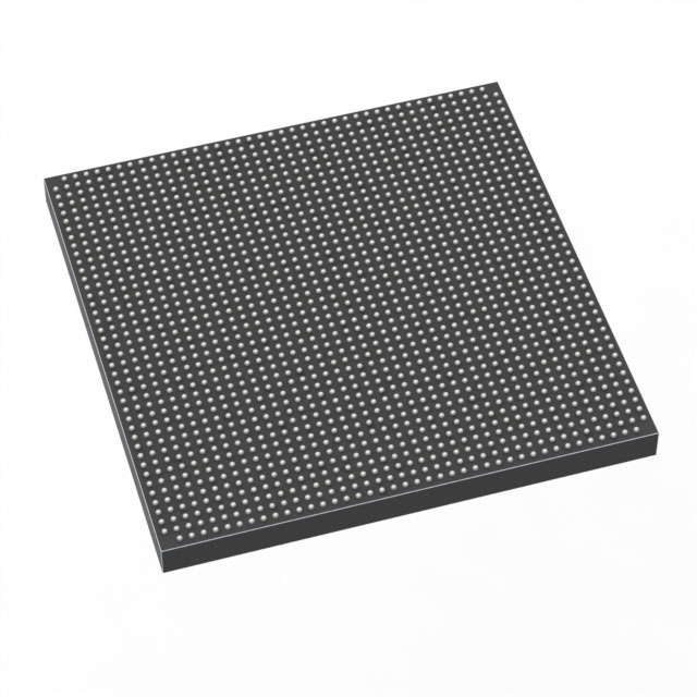
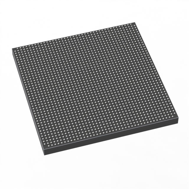
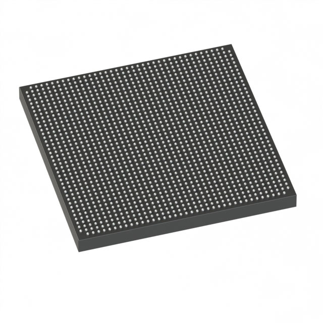
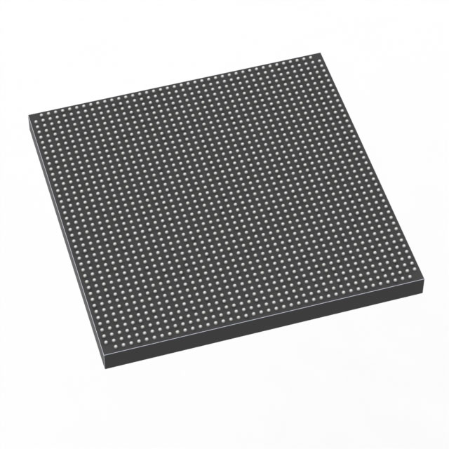
Overview of 5SGXEB5R2F40C1G – Stratix® V GX Field Programmable Gate Array (FPGA) IC, 490,000 logic elements, approximately 42 Mbits RAM, 432 I/Os, 1517-FBGA (40×40)
The 5SGXEB5R2F40C1G is an Intel Stratix V GX family FPGA offering very high logic density and on-chip memory for complex, programmable hardware implementations. As a member of the Stratix V GX family, this device targets designs that require extensive logic resources, substantial embedded RAM, and high I/O count while operating within a commercial temperature range.
Key device electrical parameters include a core supply window of 870 mV to 930 mV and an operating temperature range of 0 °C to 85 °C. The device is supplied in a 1517-FBGA (40×40) surface-mount package and is RoHS compliant.
Key Features
- Core Capacity 490,000 logic elements for implementing large-scale programmable logic and custom hardware architectures.
- Embedded Memory Approximately 42 Mbits of on-chip RAM to support deep buffering, LUT-based storage, and memory-intensive algorithms.
- I/O Density 432 I/O pins in a 1517-FBGA (40×40) package to support complex multi-interface designs and board-level integration.
- Transceiver Capability (Stratix V GX family) Stratix V GX devices include high-speed transceiver options; the family supports transceiver speed grades up to 14.1 Gbps depending on the selected speed grade.
- Power and Supply Core voltage support from 870 mV to 930 mV, providing the defined operating window for reliable device operation.
- Package & Mounting 1517-FBGA (40×40) supplier device package with surface-mount mounting type for standard PCB assembly processes.
- Commercial Temperature Grade Rated for operation from 0 °C to 85 °C for mainstream commercial applications.
- Regulatory Compliance RoHS compliant.
Typical Applications
- Custom hardware acceleration Large logic capacity and substantial embedded RAM enable implementation of application-specific accelerators and compute pipelines.
- High-density I/O systems 432 I/Os support multi-protocol interfacing, board-level aggregation, and complex host or peripheral connectivity.
- High-bandwidth serial links Stratix V GX family transceiver capabilities (depending on speed grade) support high-speed serial communications and link aggregation tasks.
- Signal and data-path processing On-chip memory and logic resources facilitate DSP, packet processing, and streaming data applications that require low-latency, programmable logic.
Unique Advantages
- High integration density: 490,000 logic elements combined with ~42 Mbits of embedded RAM reduce reliance on external logic and memory, simplifying system BOMs.
- Extensive I/O capability: 432 I/Os in a compact FBGA package enable high connector counts and diverse interface options on a single device.
- Family-level transceiver support: Stratix V GX family transceiver speed grades provide options for high-speed serial links tailored to system bandwidth requirements.
- Defined power envelope: Core supply range of 870–930 mV gives precise electrical constraints for power-supply design and thermal planning.
- Commercial-ready packaging and compliance: Surface-mount 1517-FBGA package and RoHS compliance support mainstream commercial production and regulatory requirements.
- Documented device characteristics: Electrical and switching characteristics, I/O timing, and operating conditions are detailed in the Stratix V device documentation for design validation.
Why Choose 5SGXEB5R2F40C1G?
The 5SGXEB5R2F40C1G combines very high logic capacity, substantial on-chip memory, and a high I/O count in a commercial-grade Stratix V GX device. It is well suited for designers who require a highly programmable platform for complex hardware acceleration, dense I/O integration, and transceiver-based serial connectivity within defined power and temperature envelopes.
Backed by Intel’s Stratix V family documentation, this device provides clear electrical and switching specifications to support design verification and system integration, making it appropriate for mainstream commercial applications where scalability and documented device behavior matter.
Request a quote or submit an inquiry to evaluate the 5SGXEB5R2F40C1G for your next design project.





















Date Founded: 1968
Headquarters: Santa Clara, California, USA
Employees: 130,000+
Revenue: $54.23 Billion
Certifications and Memberships: ISO9001:2015, ISO14001:2015, ISO17025:2017, ISO27001:2022, ISO45001:2018, ISO50001:2018


