
5SGXEB5R2F40C2G
| Part Description |
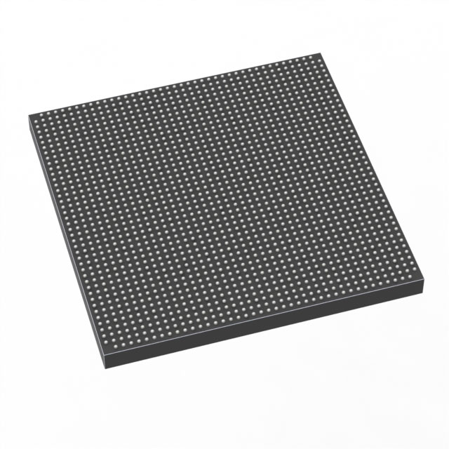
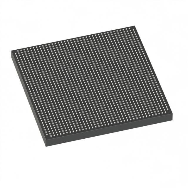
Stratix® V GX Field Programmable Gate Array (FPGA) IC 432 41984000 490000 1517-FBGA (40x40) |
|---|---|
| Quantity | 690 Available (as of June 16, 2026) |

| Product Category | Field Programmable Gate Array (FPGA) |
|---|---|
| Manufacturer | Intel |
| Manufacturing Status | Active |
| Manufacturer Standard Lead Time | 26 Weeks |
| Datasheet |
Specifications & Environmental
| Device Package | 1517-FBGA (40x40) | Grade | Commercial | Operating Temperature | 0°C – 85°C | ||
|---|---|---|---|---|---|---|---|
| Package / Case | 1517-FBGA (40x40) | Number of I/O | 432 | Voltage | 870 mV - 930 mV | ||
| Mounting Method | Surface Mount | RoHS Compliance | RoHS Compliant | REACH Compliance | REACH Unaffected | ||
| Moisture Sensitivity Level | 3 (168 Hours) | Number of LABs/CLBs | 185000 | Number of Logic Elements/Cells | 490000 | ||
| Number of Gates | N/A | ECCN | N/A | HTS Code | N/A | ||
| Qualification | N/A | Total RAM Bits | 41984000 |
Overview of 5SGXEB5R2F40C2G – Stratix® V GX FPGA, 490,000 logic elements, 432 I/O (1517‑FBGA)
The 5SGXEB5R2F40C2G is an Intel Stratix® V GX field programmable gate array (FPGA) in a 1517‑FBGA (40×40) surface‑mount package. It provides high logic density and large on‑chip memory capacity for complex digital designs that require substantial I/O and embedded RAM resources.
Targeted for commercial applications, this device combines up to 490,000 logic elements, approximately 42 Mbits of embedded memory, and 432 user I/O to support intensive data buffering, parallel processing, and high‑density integration in system‑level designs.
Key Features
- Core Logic Up to 490,000 logic elements to implement large-scale digital functions and deep datapaths.
- Embedded Memory Approximately 42 Mbits of on‑chip RAM for buffering, lookup tables, and on‑chip storage.
- I/O Density 432 user I/O pins to support broad connectivity and system interfacing requirements.
- Power and Supply Operates with a core voltage supply range of 870 mV to 930 mV to meet device power rail requirements.
- Package and Mounting 1517‑FBGA (40×40) surface‑mount package for compact board integration and high pin count.
- Commercial Temperature Grade Rated for operation from 0 °C to 85 °C for commercial‑grade deployment.
- Regulatory Compliance RoHS compliant.
Typical Applications
- High‑density signal processing Implement large parallel processing engines and custom datapaths using the device's extensive logic resources and embedded RAM.
- System I/O aggregation Aggregate and route large numbers of signals with 432 I/O for system controllers, protocol bridges, or instrumentation front ends.
- On‑chip buffering and memory‑intensive tasks Use approximately 42 Mbits of embedded RAM for packet buffering, FIFOs, and lookup tables within complex designs.
Unique Advantages
- High logic capacity: 490,000 logic elements enable consolidation of multiple functions into a single device, reducing board‑level component count.
- Significant embedded memory: Approximately 42 Mbits of RAM supports data‑intensive operations without relying on external memory for many tasks.
- Extensive I/O support: 432 I/O pins provide flexibility for dense system interfacing and parallel signal paths.
- Compact, high‑pin package: The 1517‑FBGA (40×40) form factor balances high pin count with compact PCB area usage for space‑constrained designs.
- Commercial temperature rating: Designed for 0 °C to 85 °C operation to meet typical commercial environment requirements.
- RoHS compliant: Conforms to RoHS requirements for environmentally conscious designs.
Why Choose 5SGXEB5R2F40C2G?
The 5SGXEB5R2F40C2G positions itself as a high‑density, memory‑capable Stratix V GX FPGA suitable for commercial applications that demand large logic arrays, substantial embedded RAM, and a high I/O count in a compact BGA package. Its combination of 490,000 logic elements, approximately 42 Mbits of on‑chip RAM, and 432 I/O makes it a strong candidate for consolidating complex system functions into a single programmable device.
Designers seeking scalability and integration in commercial systems will find this device appropriate for advanced processing, buffering, and interfacing tasks while benefiting from Intel’s Stratix V family documentation and device electrical characteristics.
Request a quote or submit an inquiry to receive pricing and availability information for 5SGXEB5R2F40C2G and to discuss how this FPGA can fit your design requirements.


Date Founded: 1968
Headquarters: Santa Clara, California, USA
Employees: 130,000+
Revenue: $54.23 Billion
Certifications and Memberships: ISO9001:2015, ISO14001:2015, ISO17025:2017, ISO27001:2022, ISO45001:2018, ISO50001:2018


