
5SGXEB5R3F43C3G
| Part Description |
Stratix® V GX Field Programmable Gate Array (FPGA) IC 600 41984000 490000 1760-BBGA, FCBGA |
|---|---|
| Quantity | 1,809 Available (as of June 14, 2026) |

| Product Category | Field Programmable Gate Array (FPGA) |
|---|---|
| Manufacturer | Intel |
| Manufacturing Status | Active |
| Manufacturer Standard Lead Time | 26 Weeks |
| Datasheet |
Specifications & Environmental
| Device Package | 1760-FCBGA (42.5x42.5) | Grade | Commercial | Operating Temperature | 0°C – 85°C | ||
|---|---|---|---|---|---|---|---|
| Package / Case | 1760-BBGA, FCBGA | Number of I/O | 600 | Voltage | 820 mV - 880 mV | ||
| Mounting Method | Surface Mount | RoHS Compliance | RoHS Compliant | REACH Compliance | REACH Unaffected | ||
| Moisture Sensitivity Level | 3 (168 Hours) | Number of LABs/CLBs | 185000 | Number of Logic Elements/Cells | 490000 | ||
| Number of Gates | N/A | ECCN | N/A | HTS Code | N/A | ||
| Qualification | N/A | Total RAM Bits | 41984000 |
Overview of 5SGXEB5R3F43C3G – Stratix® V GX FPGA IC, 600 I/O, 1760-BBGA
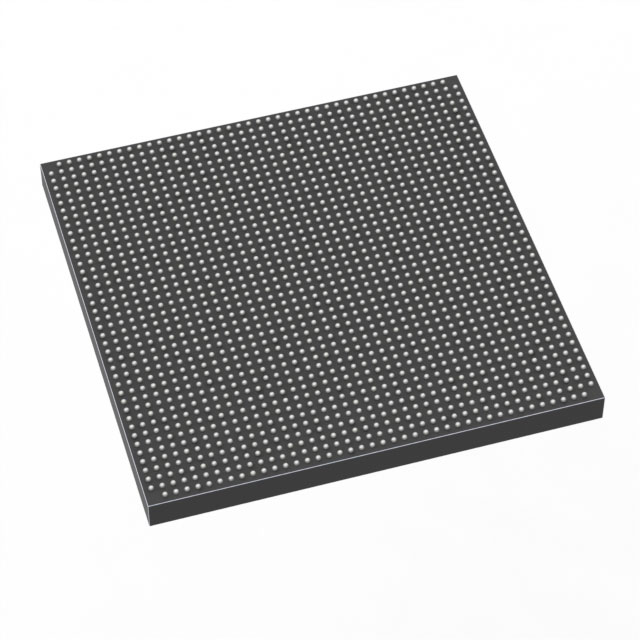
The 5SGXEB5R3F43C3G is an Intel Stratix® V GX field-programmable gate array (FPGA) in a 1760-ball FCBGA package. This commercial-grade, surface-mount device provides a high-density programmable fabric with a large I/O count and substantial on-chip memory for complex digital designs.
With 490,000 logic elements, approximately 42 Mbits of embedded memory, and up to 600 I/O pins, this Stratix V GX device is targeted at high-performance systems requiring dense logic, extensive I/O connectivity, and low-voltage core operation (820 mV–880 mV).
Key Features
- Core Logic 490,000 logic elements (LEs) for large-scale programmable logic and complex system integration.
- Embedded Memory Approximately 42 Mbits of on-chip RAM to support data buffering, lookup tables, and state storage within the FPGA fabric.
- I/O Density Up to 600 user I/O pins to accommodate wide parallel interfaces and multiple high-speed connectivity channels.
- Package & Mounting 1760-BBGA (1760-FCBGA) package, supplier package size 42.5 × 42.5 mm; surface-mount assembly.
- Power & Voltage Core voltage supply range: 820 mV to 880 mV to match low-voltage system designs.
- Operating Range Commercial temperature grade with operating temperature from 0 °C to 85 °C.
- Standards & Compliance RoHS compliant.
- Stratix V GX Family Context As part of the Stratix V GX family, the series documentation includes transceiver speed grade information and detailed electrical characteristics for system-level design and power planning.
Typical Applications
- High‑speed communications Large I/O and Stratix V GX family transceiver capabilities make the device suitable for networking and communications subsystems requiring multi-channel connectivity.
- Data processing and acceleration High logic density and substantial embedded memory support compute-heavy data-paths, streaming processors, and protocol offload engines.
- Test & measurement systems Wide I/O and flexible fabric enable custom digital front ends, real-time signal processing, and multi-channel instrumentation.
Unique Advantages
- High integration density: 490,000 logic elements and approximately 42 Mbits of RAM reduce the need for external logic and memory, simplifying BOM and board routing.
- Extensive I/O capability: Up to 600 I/O pins allow direct interfacing to many peripherals and high-pin-count subsystems without dense connector wiring or multiplexing.
- Low-voltage core operation: 820 mV–880 mV core supply supports modern low-voltage system architectures while enabling efficient power planning.
- Commercial-grade thermal envelope: Rated for 0 °C to 85 °C operation to meet standard commercial deployment requirements.
- RoHS compliant: Conforms to RoHS directives for environmentally responsible designs.
Why Choose 5SGXEB5R3F43C3G?
The 5SGXEB5R3F43C3G combines a high count of logic elements and embedded memory with broad I/O capability and a large FCBGA package to support demanding, densely integrated FPGA designs. Its commercial-grade specification and documented Stratix V GX family electrical characteristics make it a practical choice for teams designing high-performance communication, processing, and test systems that require scalable programmable logic.
Engineers and procurement teams seeking a high-density, low-voltage FPGA with extensive I/O and on-chip memory will find this device suited to complex system integration and rapid prototyping within commercial operating environments.
Request a quote or submit an inquiry to receive pricing and availability for the 5SGXEB5R3F43C3G.


Date Founded: 1968
Headquarters: Santa Clara, California, USA
Employees: 130,000+
Revenue: $54.23 Billion
Certifications and Memberships: ISO9001:2015, ISO14001:2015, ISO17025:2017, ISO27001:2022, ISO45001:2018, ISO50001:2018


