
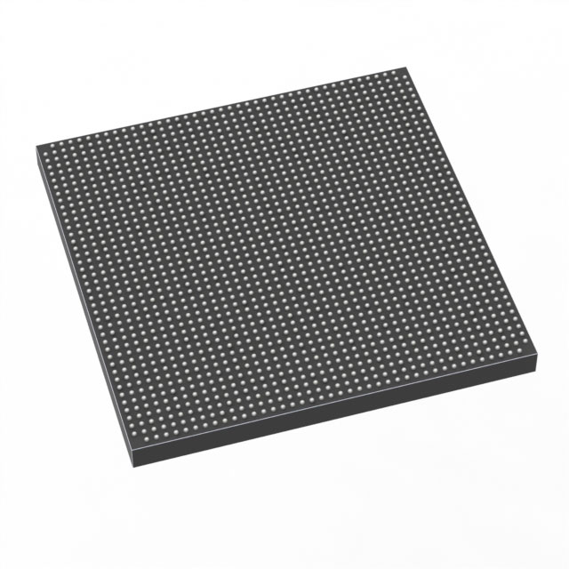
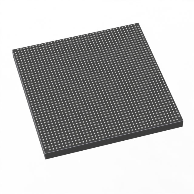
5SGXEB5R3F43C3
| Part Description |
Stratix® V GX Field Programmable Gate Array (FPGA) IC 600 41984000 490000 1760-BBGA, FCBGA |
|---|---|
| Quantity | 480 Available (as of October 7, 2026) |
| Product Category | Field Programmable Gate Array (FPGA) |
|---|---|
| Manufacturer | Intel |
| Manufacturing Status | Obsolete |
| Manufacturer Standard Lead Time | Contact Us |
| Datasheet |
Specifications & Environmental
| Device Package | 1760-FCBGA (42.5x42.5) | Grade | Commercial | Operating Temperature | 0°C – 85°C | ||
|---|---|---|---|---|---|---|---|
| Package / Case | 1760-BBGA, FCBGA | Number of I/O | 600 | Voltage | 820 mV - 880 mV | ||
| Mounting Method | Surface Mount | RoHS Compliance | RoHS Compliant | REACH Compliance | REACH Unknown | ||
| Moisture Sensitivity Level | 3 (168 Hours) | Number of LABs/CLBs | 185000 | Number of Logic Elements/Cells | 490000 | ||
| Number of Gates | N/A | ECCN | OBSOLETE | HTS Code | N/A | ||
| Qualification | N/A | Total RAM Bits | 41984000 |
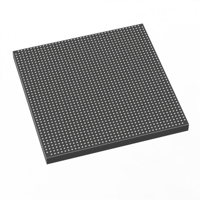
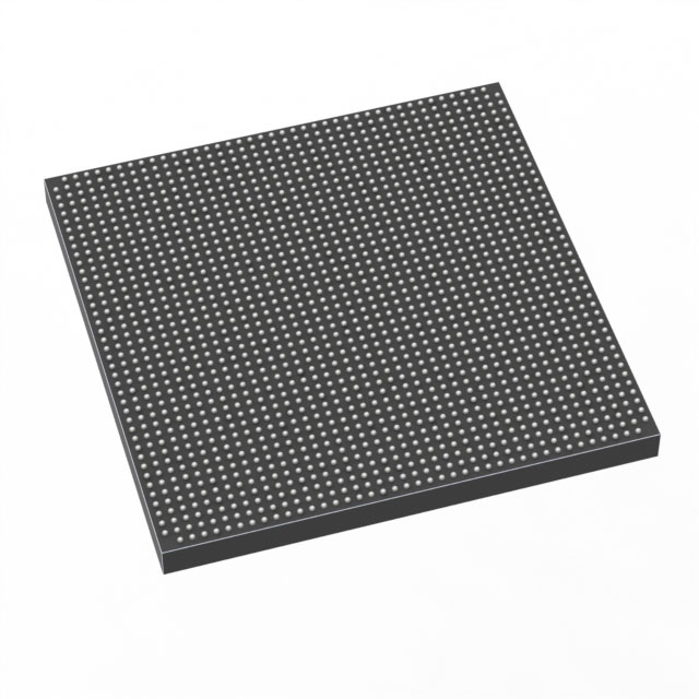
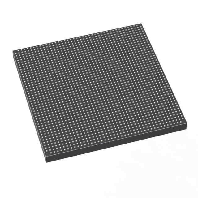
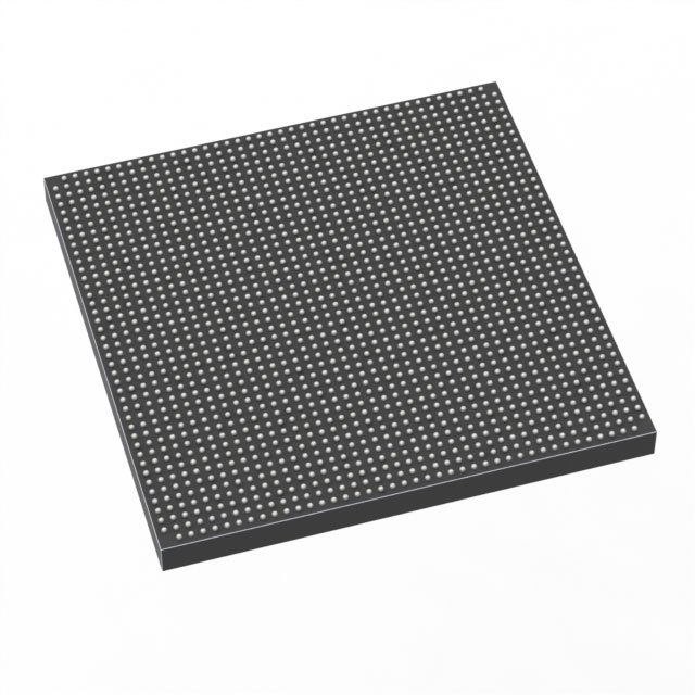
Overview of 5SGXEB5R3F43C3 – Stratix® V GX Field Programmable Gate Array (FPGA), 1760-FCBGA
The 5SGXEB5R3F43C3 is a Stratix® V GX family FPGA from Intel configured in a 1760-FCBGA package. It delivers very high logic density, substantial on‑chip memory, and a large I/O count for complex digital designs.
Targeted at applications that require extensive programmable logic, significant embedded RAM, and broad connectivity, this commercial‑grade device provides a combination of integration and scalability for advanced system designs.
Key Features
- High Logic Density Approximately 490,000 logic elements to implement large, complex designs and high‑gate‑count functions.
- Embedded Memory Approximately 42 Mbits of on‑chip RAM for buffering, FIFOs, and data‑intensive processing tasks.
- Extensive I/O Up to 600 user I/O pins to support wide parallel interfaces, multiple peripherals, and high‑pin‑count daughtercard connections.
- Core Voltage Operates with a core supply in the 820 mV to 880 mV range, consistent with modern FPGA core‑voltage requirements.
- Package & Mounting 1760‑FCPBGA (1760‑FCBGA / 1760‑BBGA) package footprint (42.5 × 42.5 mm) in a surface‑mount form factor for dense board integration.
- Commercial Temperature Grade Rated for 0 °C to 85 °C operation for standard commercial applications.
- Standards Compliance RoHS compliant to support current environmental and manufacturing requirements.
- Family Documentation Part of the Stratix V GX device family with published electrical and switching characteristics covering operating conditions, power, and I/O timing.
Typical Applications
- Complex digital systems — For large FPGA designs that require approximately 490,000 logic elements and substantial embedded memory to implement high‑gate‑count logic and deep buffering.
- High‑I/O interfacing — Suitable where up to 600 I/Os are needed for multiple parallel buses, external memory interfaces, or dense peripheral connectivity.
- Data buffering and processing — The ~42 Mbits of on‑chip RAM supports significant on‑device data storage and streaming applications.
Unique Advantages
- High integration density: Nearly half a million logic elements reduce the need for multiple devices and simplify system partitioning.
- Large embedded memory: Approximately 42 Mbits of RAM enables on‑chip buffering and state storage without external memory for many designs.
- Broad I/O capability: 600 available I/Os support complex interfacing and flexible board‑level connectivity options.
- Compact FCBGA package: 1760‑FCBGA (42.5 × 42.5 mm) provides a high‑pin‑count solution in a standardized surface‑mount form factor.
- Commercial operating range: 0 °C to 85 °C rating aligns with standard commercial product requirements and deployment.
- RoHS compliant: Complies with current lead‑free and restricted substance requirements for manufacturability.
Why Choose 5SGXEB5R3F43C3?
The 5SGXEB5R3F43C3 combines substantial programmable logic resources, large on‑chip RAM, and a high I/O count in a single commercial‑grade Stratix V GX FPGA package. Its core voltage range and package density make it well suited for designs that demand integration and scalability without partitioning across multiple devices.
This device is appropriate for teams building advanced digital systems that need significant internal memory and I/O capability while maintaining a compact PCB footprint. As part of the Stratix V family, it is supported by published device documentation covering electrical characteristics, switching behavior, and I/O timing for reliable hardware design and validation.
Request a quote or submit a sales inquiry to receive pricing, availability, and ordering information for the 5SGXEB5R3F43C3.





















Date Founded: 1968
Headquarters: Santa Clara, California, USA
Employees: 130,000+
Revenue: $54.23 Billion
Certifications and Memberships: ISO9001:2015, ISO14001:2015, ISO17025:2017, ISO27001:2022, ISO45001:2018, ISO50001:2018


