
5SGXEB5R3F43I4
| Part Description |
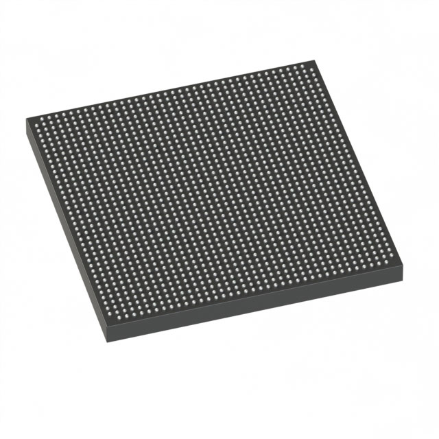
Stratix® V GX Field Programmable Gate Array (FPGA) IC 600 41984000 490000 1760-BBGA, FCBGA |
|---|---|
| Quantity | 284 Available (as of June 14, 2026) |

| Product Category | Field Programmable Gate Array (FPGA) |
|---|---|
| Manufacturer | Intel |
| Manufacturing Status | Obsolete |
| Manufacturer Standard Lead Time | Contact Us |
| Datasheet |
Specifications & Environmental
| Device Package | 1760-FCBGA (42.5x42.5) | Grade | Industrial | Operating Temperature | -40°C – 100°C | ||
|---|---|---|---|---|---|---|---|
| Package / Case | 1760-BBGA, FCBGA | Number of I/O | 600 | Voltage | 820 mV - 880 mV | ||
| Mounting Method | Surface Mount | RoHS Compliance | RoHS Compliant | REACH Compliance | REACH Unknown | ||
| Moisture Sensitivity Level | 3 (168 Hours) | Number of LABs/CLBs | 185000 | Number of Logic Elements/Cells | 490000 | ||
| Number of Gates | N/A | ECCN | OBSOLETE | HTS Code | N/A | ||
| Qualification | N/A | Total RAM Bits | 41984000 |
Overview of 5SGXEB5R3F43I4 – Stratix® V GX Field Programmable Gate Array (FPGA) IC 600 41984000 490000 1760-BBGA, FCBGA
The 5SGXEB5R3F43I4 is a high-density Stratix V GX FPGA from Intel, delivered in a 1760‑pin FCBGA package. It provides substantial on-chip logic and memory capacity together with a large I/O count for demanding industrial applications.
With approximately 490,000 logic elements, roughly 42 Mbits of embedded memory, and 600 I/O pins, this industrial‑grade device is suited to designs that require extensive logic integration, significant embedded RAM, and broad external connectivity while operating across a wide industrial temperature range.
Key Features
- Core Logic Approximately 490,000 logic elements provide high integration density for complex digital designs and large-scale custom logic implementations.
- Embedded Memory Total on-chip RAM of 41,984,000 bits (approximately 42 Mbits) for buffering, packet processing, and local data storage without external memory dependency.
- I/O Capacity 600 general-purpose I/O pins support wide external interfacing and parallel connectivity for multi‑lane or multi‑peripheral systems.
- Package and Mounting 1760‑FBGA (1760‑FCBGA, 42.5 × 42.5 mm) surface-mount package for high pin-count, board-level integration in compact footprints.
- Voltage and Power Core supply range specified at 820 mV to 880 mV to match system power rail requirements for this device.
- Industrial Temperature Grade Rated for operation from −40 °C to 100 °C for deployment in industrial environments.
- Compliance RoHS compliant to meet regulatory environmental requirements.
- Stratix V GX Family Characteristics As a member of the Stratix V GX family, the device aligns with family-level transceiver speed grade offerings described in the series documentation.
Typical Applications
- High‑performance networking and communications Large logic capacity and high I/O count enable implementations of packet processing, switching, and protocol adaptation functions.
- Data throughput and acceleration Substantial embedded RAM and logic density support buffering, stream processing, and hardware acceleration tasks in compute‑intensive systems.
- Industrial control and automation Industrial temperature rating and extensive I/O make the device suitable for complex control systems, motor drives, and sensor aggregation.
- Prototyping and complex system integration High logic element count and FCBGA pinout facilitate system‑level prototyping and integration of multiple subsystems on a single FPGA.
Unique Advantages
- High integration density: Large logic element count reduces the need for multiple devices and simplifies system architecture.
- Substantial on‑chip memory: Approximately 42 Mbits of embedded RAM supports deep buffering and local data processing without external memory overhead.
- Extensive external connectivity: 600 I/O pins allow flexible interfacing to high‑pin-count peripherals and multi‑lane interconnects.
- Industrial robustness: Rated for −40 °C to 100 °C operation, addressing a wide range of industrial deployment environments.
- High‑pin FCBGA package: 1760‑pin FCBGA (42.5 × 42.5 mm) enables maximum I/O and signal routing density for advanced board designs.
- Controlled core voltage range: Specified 820–880 mV supply enables predictable core power planning and thermal design.
Why Choose 5SGXEB5R3F43I4?
This Stratix V GX FPGA delivers a combination of high logic capacity, substantial embedded memory, and broad I/O availability in an industrial‑grade FCBGA package. It is positioned for projects that require consolidation of complex digital functions, local data buffering, and extensive external interfacing within temperature‑challenging environments.
Designers seeking a scalable, high‑density FPGA solution for industrial communications, data processing, or system integration will find the 5SGXEB5R3F43I4 aligns with those needs while providing the predictable supply and thermal parameters required for robust hardware design.
Request a quote or submit an inquiry to receive pricing, lead‑time, and availability information for the 5SGXEB5R3F43I4.


Date Founded: 1968
Headquarters: Santa Clara, California, USA
Employees: 130,000+
Revenue: $54.23 Billion
Certifications and Memberships: ISO9001:2015, ISO14001:2015, ISO17025:2017, ISO27001:2022, ISO45001:2018, ISO50001:2018


