
5SGXMA5N2F45C1N
| Part Description |
Stratix® V GX Field Programmable Gate Array (FPGA) IC 840 46080000 490000 1932-BBGA, FCBGA |
|---|---|
| Quantity | 5 Available (as of June 15, 2026) |

| Product Category | Field Programmable Gate Array (FPGA) |
|---|---|
| Manufacturer | Intel |
| Manufacturing Status | Obsolete |
| Manufacturer Standard Lead Time | Contact Us |
| Datasheet |
Specifications & Environmental
| Device Package | 1932-FBGA, FC (45x45) | Grade | Commercial | Operating Temperature | 0°C – 85°C | ||
|---|---|---|---|---|---|---|---|
| Package / Case | 1932-BBGA, FCBGA | Number of I/O | 840 | Voltage | 870 mV - 930 mV | ||
| Mounting Method | Surface Mount | RoHS Compliance | RoHS Compliant | REACH Compliance | REACH Unknown | ||
| Moisture Sensitivity Level | 3 (168 Hours) | Number of LABs/CLBs | 185000 | Number of Logic Elements/Cells | 490000 | ||
| Number of Gates | N/A | ECCN | 3A001A2C | HTS Code | 8542.39.0001 | ||
| Qualification | N/A | Total RAM Bits | 46080000 |
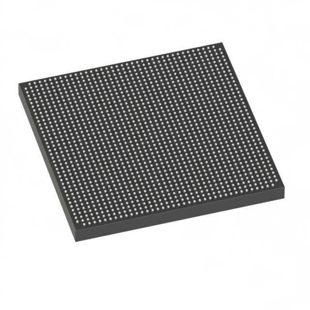
Overview of 5SGXMA5N2F45C1N – Stratix® V GX FPGA, 490,000 logic elements, 1932-BBGA
The 5SGXMA5N2F45C1N is a Stratix® V GX Field Programmable Gate Array (FPGA) IC in a 1932-BBGA (FCBGA) package. It delivers high-density programmable logic with 490,000 logic elements and approximately 46 Mbits of embedded memory for complex, resource-intensive designs.
With 840 I/O pins, a surface-mount 1932-FBGA (45×45) package, and a commercial operating temperature range of 0 °C to 85 °C, this device is designed for applications that require significant on-chip routing, memory, and I/O capacity while operating at a core voltage between 870 mV and 930 mV.
Key Features
- Core Logic 490,000 logic elements provide extensive programmable logic capacity for complex digital designs.
- Embedded Memory Approximately 46 Mbits of on-chip RAM to support large data buffers, lookup tables, and state storage.
- I/O and Interface Density 840 user I/O pins for wide connectivity and flexible system interfacing.
- Package & Mounting 1932-BBGA (FCBGA) package; supplier device package listed as 1932-FBGA, FC (45×45); surface-mount mounting type.
- Power Core supply operating range of 870 mV to 930 mV for the device core rails.
- Temperature Grade Commercial grade device with an operating temperature range of 0 °C to 85 °C.
- Compliance RoHS compliant.
- Series-Level Notes Stratix V GX devices are provided in a range of core and transceiver speed grades at the series level (refer to the Stratix V device documentation for series options).
Typical Applications
- High-density digital processing For designs that need large logic capacity and embedded memory to implement complex algorithms and state machines.
- High I/O systems Systems requiring extensive external connectivity benefit from the device’s 840 I/O pins for parallel interfaces and board-level routing.
- Data buffering and on-chip storage Applications that require substantial on-chip RAM for buffering, lookup tables, and temporary data storage.
- Platform and system integration Dense FPGA logic and large memory resources make the device suitable for integrating multiple functions onto a single programmable device.
Unique Advantages
- High logic capacity: 490,000 logic elements enable large-scale integration of custom logic and complex functions on-chip.
- Substantial embedded memory: Approximately 46 Mbits of RAM reduce external memory dependence and simplify board-level BOM.
- Extensive I/O resources: 840 I/O pins provide flexibility for multi-interface designs and high pin-count peripherals.
- Compact, production-ready package: 1932-FBGA (45×45) surface-mount package supports high-density PCB designs.
- Commercial temperature rating: Specified 0 °C to 85 °C operating range for standard commercial applications.
- Regulatory compliance: RoHS compliant to support lead-free manufacturing and regulatory requirements.
Why Choose 5SGXMA5N2F45C1N?
The 5SGXMA5N2F45C1N positions itself as a high-density Stratix V GX FPGA option for designs that demand large programmable logic resources, significant on-chip RAM, and broad I/O capacity in a single package. Its combination of 490,000 logic elements, approximately 46 Mbits of embedded memory, and 840 I/O pins enables consolidation of complex system functions and reduces reliance on external components.
This commercial-grade device is suited to engineering teams looking to deploy feature-rich, scalable FPGA-based solutions with clear power and thermal characteristics (870 mV–930 mV core supply, 0 °C–85 °C operating range) and RoHS compliance for modern production environments.
Request a quote or submit an inquiry to receive pricing, availability, and additional technical information for 5SGXMA5N2F45C1N.


Date Founded: 1968
Headquarters: Santa Clara, California, USA
Employees: 130,000+
Revenue: $54.23 Billion
Certifications and Memberships: ISO9001:2015, ISO14001:2015, ISO17025:2017, ISO27001:2022, ISO45001:2018, ISO50001:2018


