
5SGXMA5N3F40C2WN
| Part Description |
Stratix® V GX Field Programmable Gate Array (FPGA) IC 600 46080000 490000 1517-BBGA, FCBGA |
|---|---|
| Quantity | 557 Available (as of June 15, 2026) |

| Product Category | Field Programmable Gate Array (FPGA) |
|---|---|
| Manufacturer | Intel |
| Manufacturing Status | Obsolete |
| Manufacturer Standard Lead Time | Contact Us |
| Datasheet |
Specifications & Environmental
| Device Package | 1517-FBGA (40x40) | Grade | Commercial | Operating Temperature | 0°C – 85°C | ||
|---|---|---|---|---|---|---|---|
| Package / Case | 1517-BBGA, FCBGA | Number of I/O | 600 | Voltage | 870 mV - 930 mV | ||
| Mounting Method | Surface Mount | RoHS Compliance | RoHS non-compliant | REACH Compliance | REACH Unknown | ||
| Moisture Sensitivity Level | 4 (72 Hours) | Number of LABs/CLBs | 185000 | Number of Logic Elements/Cells | 490000 | ||
| Number of Gates | N/A | ECCN | OBSOLETE | HTS Code | N/A | ||
| Qualification | N/A | Total RAM Bits | 46080000 |
Overview of 5SGXMA5N3F40C2WN – Stratix® V GX Field Programmable Gate Array (FPGA)
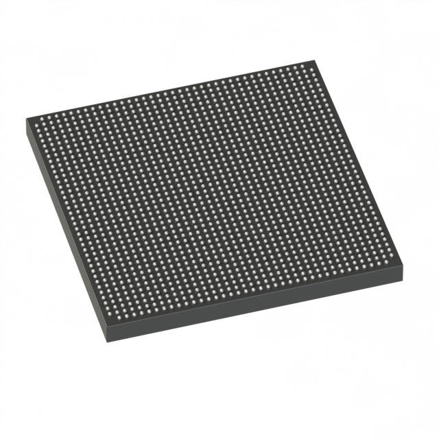
The 5SGXMA5N3F40C2WN is a Stratix V GX family FPGA delivered in a 1517-BBGA FCBGA package for surface-mount assembly. It provides a high-density programmable fabric with large on-chip memory and extensive I/O capacity suitable for commercial-temperature designs.
This device targets designs that require large logic capacity, substantial embedded RAM, and broad board-level connectivity while operating within a commercial temperature range. Core power rails operate between 870 mV and 930 mV, enabling designers to plan power delivery precisely.
Key Features
- Core capacity — Approximately 490,000 logic elements and 185,000 logic blocks for complex logic integration and high-density implementations.
- Embedded memory — Approximately 46 Mbits of on-chip RAM to support large data buffering and state storage without external memory in many use cases.
- I/O resources — 600 dedicated I/O pins to support extensive peripheral and board-level interfacing.
- Power — Core supply voltage range of 870 mV to 930 mV for accurate power budgeting and regulator selection.
- Package and mounting — 1517-BBGA (1517-FBGA, 40×40) FCBGA package in a surface-mount form factor for compact board layouts.
- Operating range — Commercial temperature grade with an operating range of 0 °C to 85 °C.
- Compliance — RoHS compliant for regulatory and manufacturing alignment.
Typical Applications
- High-density logic integration — Deploy the device where large numbers of logic elements and logic blocks are required to implement complex digital functions on a single FPGA.
- Embedded memory–intensive designs — Use the device’s approximately 46 Mbits of on-chip RAM for buffering, packet processing, and other memory-heavy functions.
- Board-level I/O aggregation — Leverage 600 I/Os to connect multiple peripherals, interfaces, and external components without immediate reliance on I/O expanders.
- Commercial embedded systems — Suitable for systems designed to operate across a 0 °C to 85 °C range where high logic density and memory are required.
Unique Advantages
- High programmable density: Approximately 490,000 logic elements provide headroom for large-scale FPGA implementations and iterative design expansion.
- Significant on-chip RAM: Approximately 46 Mbits of embedded memory reduces dependence on external memory for many buffering and state-storage tasks.
- Extensive I/O capacity: 600 I/O pins enable complex interfacing and reduce the need for external multiplexing or expansion.
- Compact FCBGA package: The 1517-BBGA (40×40) package supports high-density board layouts while remaining surface-mount compatible.
- Predictable power envelope: A defined core voltage range (870–930 mV) simplifies regulator selection and power-supply design.
- Commercial-temperature qualification: Rated for 0 °C to 85 °C operation to match standard commercial embedded product requirements.
Why Choose 5SGXMA5N3F40C2WN?
The 5SGXMA5N3F40C2WN combines substantial logic density, significant embedded RAM, and a high I/O count in a compact FCBGA package for commercial-temperature FPGA applications. As a member of the Stratix V GX family, it aligns with the Stratix V device ecosystem and datasheet-defined operating characteristics and speed-grade options.
This device is well suited to engineering teams that need a high-capacity, on-chip solution for complex digital processing, heavy buffering, and broad interface requirements while maintaining predictable power and thermal constraints for commercial deployments.
Request a quote or submit an inquiry to evaluate how 5SGXMA5N3F40C2WN can fit into your next design project.


Date Founded: 1968
Headquarters: Santa Clara, California, USA
Employees: 130,000+
Revenue: $54.23 Billion
Certifications and Memberships: ISO9001:2015, ISO14001:2015, ISO17025:2017, ISO27001:2022, ISO45001:2018, ISO50001:2018


