
5SGXMA7H1F35C2LN
| Part Description |
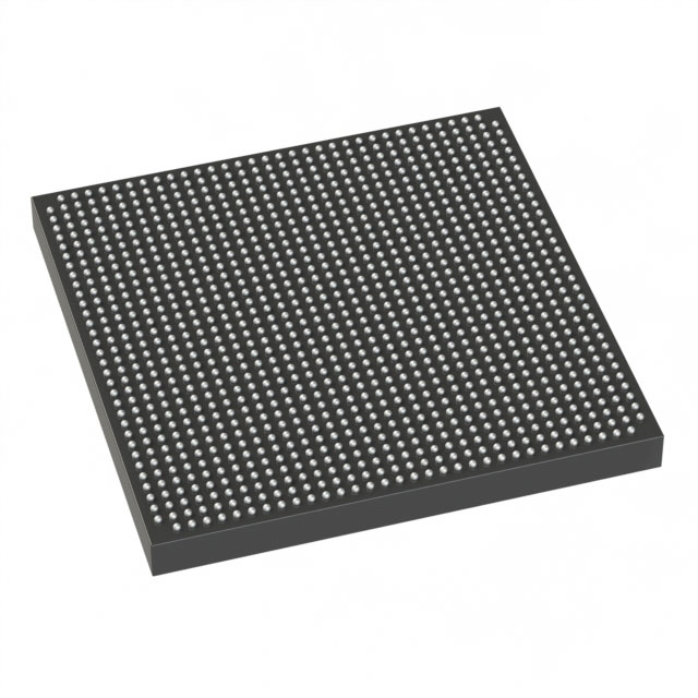
Stratix® V GX Field Programmable Gate Array (FPGA) IC 552 51200000 622000 1152-BBGA, FCBGA |
|---|---|
| Quantity | 891 Available (as of June 15, 2026) |

| Product Category | Field Programmable Gate Array (FPGA) |
|---|---|
| Manufacturer | Intel |
| Manufacturing Status | Obsolete |
| Manufacturer Standard Lead Time | Contact Us |
| Datasheet |
Specifications & Environmental
| Device Package | 1152-FBGA (35x35) | Grade | Commercial | Operating Temperature | 0°C – 85°C | ||
|---|---|---|---|---|---|---|---|
| Package / Case | 1152-BBGA, FCBGA | Number of I/O | 552 | Voltage | 820 mV - 880 mV | ||
| Mounting Method | Surface Mount | RoHS Compliance | RoHS Compliant | REACH Compliance | REACH Unknown | ||
| Moisture Sensitivity Level | 3 (168 Hours) | Number of LABs/CLBs | 234720 | Number of Logic Elements/Cells | 622000 | ||
| Number of Gates | N/A | ECCN | 3A001A2C | HTS Code | 8542.39.0001 | ||
| Qualification | N/A | Total RAM Bits | 51200000 |
Overview of 5SGXMA7H1F35C2LN – Stratix® V GX FPGA, 622,000 logic elements
The 5SGXMA7H1F35C2LN is a Stratix® V GX Field Programmable Gate Array (FPGA) in a 1152-BBGA FCBGA package, designed for high-density, high-performance digital designs. As a member of the Stratix V GX family, the device benefits from the series' documented electrical and switching characteristics and is offered in commercial temperature grade.
With 622,000 logic elements, approximately 51.2 Mbits of embedded memory, and 552 general-purpose I/O pins, this device targets complex logic integration and multi‑function system designs that require extensive on-chip resources and flexible I/O connectivity.
Key Features
- Core Capacity 622,000 logic elements provide large-scale programmable logic for complex algorithms, parallel processing, and custom datapaths.
- Embedded Memory Approximately 51.2 Mbits of on‑chip RAM to support large buffers, FIFOs, and data storage close to logic.
- High I/O Count 552 I/O pins enable dense board-level interfacing for multi-channel systems and extensive peripheral connectivity.
- Package 1152-BBGA (FCBGA), supplier package 1152-FBGA (35×35) for high‑pin‑count, compact board implementations.
- Power Supply Core voltage operating range 820 mV to 880 mV, enabling designs that target the specified core operating window.
- Operating Temperature Commercial grade operation specified from 0 °C to 85 °C.
- Mounting Surface mount device suitable for standard SMT assembly processes.
- Standards Compliance RoHS compliant.
Typical Applications
- High‑density digital processing Large logic capacity and abundant on‑chip RAM make the device suitable for custom accelerators, DSP pipelines, and FPGA-based compute blocks.
- Multi‑I/O system integration High pin count supports complex board-level interfaces, aggregation of multiple peripherals, and dense mezzanine connections.
- Multi‑channel buffering and packet handling Substantial embedded memory supports large buffering and packet processing in communications and networking subsystems.
Unique Advantages
- Substantial programmable logic: 622,000 logic elements enable consolidation of multiple functions into a single FPGA, reducing PCB complexity.
- Large on‑chip memory: Approximately 51.2 Mbits of RAM reduces dependence on external memory for many buffering and storage tasks, improving latency and simplifying routing.
- Extensive I/O resources: 552 I/O pins provide flexibility for interfacing with numerous high‑pin-count peripherals and multi‑lane designs.
- High‑pin FCBGA package: The 1152‑FBGA (35×35) package supports high interconnect density while maintaining a compact board footprint.
- Commercial temperature grade: Specified operation from 0 °C to 85 °C suits a wide range of mainstream electronics applications.
- Documented platform: Backed by Stratix V family documentation covering electrical and switching characteristics to aid system design and validation.
Why Choose 5SGXMA7H1F35C2LN?
The 5SGXMA7H1F35C2LN combines large programmable logic capacity, sizeable integrated memory, and a high number of I/O in a compact 1152‑BBGA package, making it a strong choice for designers consolidating multiple functions into a single FPGA. Its commercial temperature rating and RoHS compliance address standard industrial manufacturing and regulatory needs.
Engineers building high‑density digital systems, multi‑channel interfaces, or designs that benefit from significant on‑chip RAM will find the device's resource set and package options well suited to reduce board complexity and streamline system integration. Documentation for the Stratix V family is available to support electrical and timing validation during development.
Request a quote or submit an inquiry to start your procurement or design evaluation process for the 5SGXMA7H1F35C2LN FPGA.


Date Founded: 1968
Headquarters: Santa Clara, California, USA
Employees: 130,000+
Revenue: $54.23 Billion
Certifications and Memberships: ISO9001:2015, ISO14001:2015, ISO17025:2017, ISO27001:2022, ISO45001:2018, ISO50001:2018


