
5SGXMA7H1F35C2G
| Part Description |
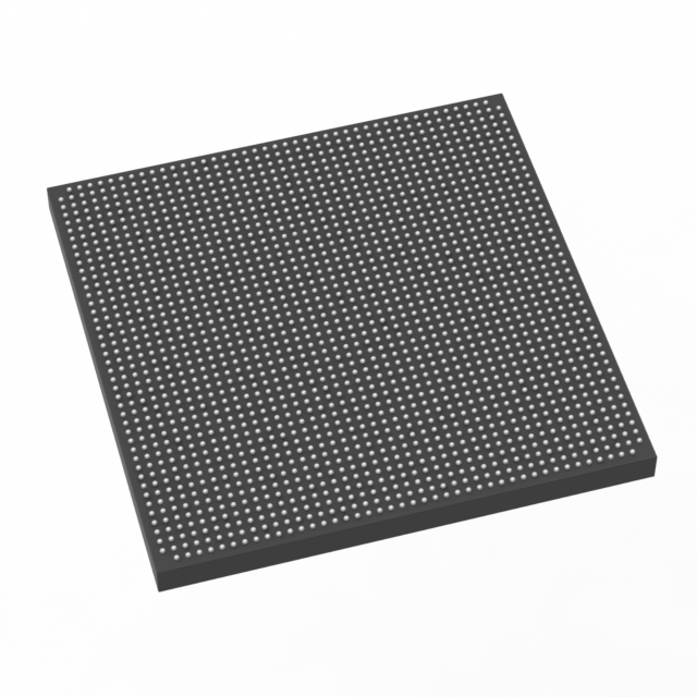
Stratix® V GX Field Programmable Gate Array (FPGA) IC 552 51200000 622000 1152-BBGA, FCBGA |
|---|---|
| Quantity | 617 Available (as of June 15, 2026) |

| Product Category | Field Programmable Gate Array (FPGA) |
|---|---|
| Manufacturer | Intel |
| Manufacturing Status | Active |
| Manufacturer Standard Lead Time | 26 Weeks |
| Datasheet |
Specifications & Environmental
| Device Package | 1152-FBGA (35x35) | Grade | Commercial | Operating Temperature | 0°C – 85°C | ||
|---|---|---|---|---|---|---|---|
| Package / Case | 1152-BBGA, FCBGA | Number of I/O | 552 | Voltage | 870 mV - 930 mV | ||
| Mounting Method | Surface Mount | RoHS Compliance | RoHS Compliant | REACH Compliance | REACH Unaffected | ||
| Moisture Sensitivity Level | 3 (168 Hours) | Number of LABs/CLBs | 234720 | Number of Logic Elements/Cells | 622000 | ||
| Number of Gates | N/A | ECCN | N/A | HTS Code | N/A | ||
| Qualification | N/A | Total RAM Bits | 51200000 |
Overview of 5SGXMA7H1F35C2G – Stratix® V GX Field Programmable Gate Array (FPGA)
The 5SGXMA7H1F35C2G is a Stratix V GX family FPGA IC from Intel designed for commercial embedded designs that require substantial on-chip logic, memory, and I/O resources. This device provides a large logic fabric, significant embedded RAM capacity, and a high I/O count in a 1152‑BBGA package, making it suitable for high-density FPGA implementations in commercial temperature environments.
Key Features
- Logic Capacity 622,000 logic elements provide a large programmable fabric for complex digital designs and extensive custom logic implementation.
- Embedded Memory Approximately 51.2 Mbits of on-chip RAM to support large buffering, packet processing, and data-path storage requirements.
- I/O Resources 552 I/O pins to accommodate wide bus interfaces, numerous peripherals, and multi‑lane connectivity on a single device.
- Package & Mounting 1152‑BBGA, FCBGA package (supplier package: 1152‑FBGA, 35×35) in a surface‑mount form factor to support compact board layouts.
- Power Core voltage supply range of 870 mV to 930 mV for device core power domains.
- Temperature & Grade Commercial grade operation with an operating range of 0 °C to 85 °C.
- Compliance RoHS compliant for regulatory environmental requirements.
Typical Applications
- High-density signal processing Utilize the 622,000 logic elements and approximately 51.2 Mbits of embedded memory to implement large-scale digital signal processing pipelines and custom accelerators.
- Complex protocol bridging High I/O count (552) enables multi-interface bridging and protocol translation on a single FPGA device.
- Large-scale control and compute Deploy extensive custom control logic and parallel compute blocks leveraging the device’s large logic and memory resources for commercial embedded systems.
Unique Advantages
- High logic and memory density: 622,000 logic elements combined with approximately 51.2 Mbits of embedded RAM support complex, memory‑intensive designs without immediate external memory dependence.
- Extensive I/O capability: 552 I/Os reduce the need for external multiplexing and simplify multi‑interface designs.
- Compact board integration: 1152‑BBGA (1152‑FBGA, 35×35) surface‑mount package enables dense PCB layouts while providing large device capacity.
- Commercial temperature suitability: Rated for 0 °C to 85 °C operation to meet a wide range of commercial deployment environments.
- Regulatory alignment: RoHS compliance supports environmental and manufacturability requirements.
- Defined core supply range: 870 mV to 930 mV core voltage specification simplifies power planning for system designers.
Why Choose 5SGXMA7H1F35C2G?
The 5SGXMA7H1F35C2G offers a combination of large logic capacity, substantial embedded memory, and a high pin count in a compact 1152‑BBGA package, tailored for commercial applications that demand dense programmable logic and abundant I/O. As a Stratix V GX family device from Intel, it aligns with device‑level electrical and switching characteristics documented for the Stratix V series.
This device is suited to design teams building scalable, compute‑ and I/O‑intensive FPGA solutions where on‑chip resources and package density are primary selection criteria.
Request a quote or submit an inquiry for 5SGXMA7H1F35C2G to discuss availability, pricing, and delivery options.


Date Founded: 1968
Headquarters: Santa Clara, California, USA
Employees: 130,000+
Revenue: $54.23 Billion
Certifications and Memberships: ISO9001:2015, ISO14001:2015, ISO17025:2017, ISO27001:2022, ISO45001:2018, ISO50001:2018


