
5SGXMA9N2F45I2LN
| Part Description |
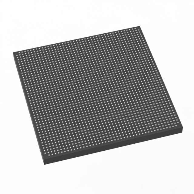
Stratix® V GX Field Programmable Gate Array (FPGA) IC 840 53248000 840000 1932-BBGA, FCBGA |
|---|---|
| Quantity | 264 Available (as of June 15, 2026) |

| Product Category | Field Programmable Gate Array (FPGA) |
|---|---|
| Manufacturer | Intel |
| Manufacturing Status | Obsolete |
| Manufacturer Standard Lead Time | Contact Us |
| Datasheet |
Specifications & Environmental
| Device Package | 1932-FBGA, FC (45x45) | Grade | Industrial | Operating Temperature | -40°C – 100°C | ||
|---|---|---|---|---|---|---|---|
| Package / Case | 1932-BBGA, FCBGA | Number of I/O | 840 | Voltage | 820 mV - 880 mV | ||
| Mounting Method | Surface Mount | RoHS Compliance | RoHS Compliant | REACH Compliance | REACH Unknown | ||
| Moisture Sensitivity Level | 3 (168 Hours) | Number of LABs/CLBs | 317000 | Number of Logic Elements/Cells | 840000 | ||
| Number of Gates | N/A | ECCN | 3A001A2C | HTS Code | 8542.39.0001 | ||
| Qualification | N/A | Total RAM Bits | 53248000 |
Overview of 5SGXMA9N2F45I2LN – Stratix® V GX FPGA, 840,000 Logic Elements, ~53.25 Mbits RAM, 840 I/O, 1932‑BBGA (FCBGA)
The 5SGXMA9N2F45I2LN is an Intel Stratix V GX field-programmable gate array supplied in a high‑pin‑count 1932‑BBGA FCBGA package. This industrial‑grade FPGA delivers large logic capacity, significant on‑chip memory, and a high number of user I/O to support complex programmable digital designs.
Targeted at designs that require high logic density, substantial embedded RAM, and broad I/O connectivity, the device provides a combination of integration and configurability for system-level implementation and high‑speed I/O requirements described for Stratix V GX family devices.
Key Features
- Logic Capacity — 840,000 logic elements to implement large-scale programmable logic and custom hardware acceleration.
- Logic Array Blocks — 317,000 logic array blocks (LABs/CLBs) for structured logic partitioning and floorplanning.
- Embedded Memory — Approximately 53.25 Mbits of on‑chip RAM for buffering, FIFOs, and data‑path storage.
- I/O Count — 840 user I/O pins to support wide parallel interfaces and multiple peripheral connections.
- Power Supply — Core voltage range of 820 mV to 880 mV to match system power delivery requirements.
- Package & Mounting — 1932‑BBGA FCBGA package (supplier device package: 1932‑FBGA, FC 45×45) with surface mount construction for high density board integration.
- Temperature & Grade — Industrial grade operation from −40 °C to 100 °C for extended operating environments.
- Environmental Compliance — RoHS compliant.
- Stratix V GX Family Characteristics — Device documentation details Stratix V GX transceiver speed grades and electrical characteristics for high‑speed serial interfaces and robust device operation.
Typical Applications
- High‑density programmable logic — Implements large custom accelerators, control logic, and glue logic where high logic element counts and on‑chip RAM are required.
- High‑speed serial interfaces — Suitable for designs leveraging the Stratix V GX family’s transceiver capabilities for high‑bandwidth communications and data links.
- System integration and prototyping — Provides ample I/O and memory for integrating multiple subsystems, evaluation platforms, and complex prototypes.
Unique Advantages
- High logic density: 840,000 logic elements support complex, large‑scale implementations without external logic expansion.
- Substantial embedded memory: Approximately 53.25 Mbits of RAM supports deep buffering, packet processing, and data‑intensive functions on‑chip.
- Extensive I/O resources: 840 I/O pins enable flexible interfacing to large parallel buses, peripherals, and mezzanine modules.
- Industrial temperature rating: −40 °C to 100 °C operation provides wider environmental tolerance for industrial deployments.
- High‑pin‑count package: 1932‑BBGA FCBGA (45×45) enables maximum routing density and connectivity for board‑level integration.
- Regulatory readiness: RoHS compliance supports environmentally conscious manufacturing processes.
Why Choose 5SGXMA9N2F45I2LN?
The 5SGXMA9N2F45I2LN positions itself as a high‑capacity Stratix V GX FPGA option for engineers who need substantial programmable logic, significant on‑chip RAM, and a large complement of I/O in an industrial‑grade package. Its combination of 840,000 logic elements, approximately 53.25 Mbits of embedded memory, and 840 I/Os makes it suited to demanding designs that require both integration density and flexible system interfacing.
With a 1932‑BBGA surface‑mount package and a defined core voltage range and temperature rating, this device offers a predictable platform for system designers seeking scalability, robust operation, and the architectural features documented for the Stratix V GX family.
Request a quote or submit an inquiry for pricing and availability for part number 5SGXMA9N2F45I2LN.


Date Founded: 1968
Headquarters: Santa Clara, California, USA
Employees: 130,000+
Revenue: $54.23 Billion
Certifications and Memberships: ISO9001:2015, ISO14001:2015, ISO17025:2017, ISO27001:2022, ISO45001:2018, ISO50001:2018


