
5SGXMABK2H40C2G
| Part Description |
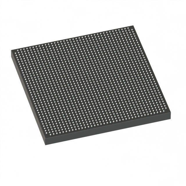
Stratix® V GX Field Programmable Gate Array (FPGA) IC 696 53248000 952000 1517-BBGA, FCBGA |
|---|---|
| Quantity | 1,505 Available (as of June 17, 2026) |

| Product Category | Field Programmable Gate Array (FPGA) |
|---|---|
| Manufacturer | Intel |
| Manufacturing Status | Active |
| Manufacturer Standard Lead Time | 26 Weeks |
| Datasheet |
Specifications & Environmental
| Device Package | 1517-HBGA (45x45) | Grade | Commercial | Operating Temperature | 0°C – 85°C | ||
|---|---|---|---|---|---|---|---|
| Package / Case | 1517-BBGA, FCBGA | Number of I/O | 696 | Voltage | 870 mV - 930 mV | ||
| Mounting Method | Surface Mount | RoHS Compliance | RoHS Compliant | REACH Compliance | REACH Unaffected | ||
| Moisture Sensitivity Level | 3 (168 Hours) | Number of LABs/CLBs | 359200 | Number of Logic Elements/Cells | 952000 | ||
| Number of Gates | N/A | ECCN | N/A | HTS Code | N/A | ||
| Qualification | N/A | Total RAM Bits | 53248000 |
Overview of 5SGXMABK2H40C2G – Stratix V GX FPGA, 952,000 Logic Elements, 1517-BBGA
The 5SGXMABK2H40C2G is a high-density Stratix® V GX Field Programmable Gate Array (FPGA) from Intel (Altera). It integrates 952,000 logic elements and approximately 53.25 Mbits of embedded memory to support complex, large-scale digital designs.
Designed for commercial-grade applications, this surface-mount FCBGA device provides extensive I/O (696 pins), on-chip memory, and a low core supply voltage range, making it suitable for multi-gigabit serial connectivity, memory-intensive processing, and large logic integration scenarios.
Key Features
- Logic Capacity — 952,000 logic elements to implement large finite-state machines, datapaths, and custom accelerators.
- Embedded Memory — Approximately 53.25 Mbits of on-chip RAM to support buffering, lookup tables, and on-chip data storage.
- I/O Density — 696 I/O pins to accommodate multiple interfaces, wide bus widths, and complex board-level interconnects.
- Core Supply Voltage — 870 mV to 930 mV supply range for core power, enabling designs that target the Stratix V GX power envelope.
- Package and Mounting — 1517-ball BGA (FCBGA / supplier package 1517-HBGA, 45×45 mm); designed for surface-mount assembly.
- Commercial Temperature Grade — Rated for 0 °C to 85 °C operation for standard commercial environments.
- Regulatory Compliance — RoHS compliant.
Typical Applications
- Multi‑Gigabit Serial Connectivity — High logic and I/O density combined with Stratix V GX transceiver family characteristics support multi‑Gbps serial interfaces and protocol bridging.
- Memory‑Intensive FPGA Designs — Large embedded RAM capacity for buffering, packet processing, and on-chip data manipulation.
- Large‑Scale Logic Integration — Implement complex control, signal-processing, or custom accelerator functions that require nearly one million logic elements.
- High‑Pin‑Count Systems — 696 I/Os enable integration with wide external buses, multiple peripherals, and board-level subsystems.
Unique Advantages
- High Logic Density: 952,000 logic elements enable consolidation of multiple functions into a single FPGA, reducing board-level complexity.
- Substantial On‑Chip Memory: Approximately 53.25 Mbits of embedded RAM help minimize external memory dependence and improve data throughput.
- Extensive I/O Capability: 696 I/Os give designers flexibility for diverse interface requirements without sacrificing routing options.
- Compact High‑Pin Package: 1517-ball FCBGA (45×45 mm) balances high density with a package form factor suited for surface-mount assembly.
- Commercial Temperature Range: Rated 0 °C to 85 °C for standard commercial deployments and controlled-environment installations.
- RoHS Compliant: Meets lead-free requirements for environmentally driven designs.
Why Choose 5SGXMABK2H40C2G?
The 5SGXMABK2H40C2G provides a high-capacity Stratix V GX FPGA solution that pairs nearly one million logic elements with substantial embedded memory and high I/O density in a single FCBGA package. Its commercial temperature rating and compact 1517-ball package make it well suited for advanced communications, compute, and data-path applications where integration and on-chip resources are priorities.
Backed by Intel (Altera) device documentation and supported design flows, this device is appropriate for development teams targeting large-scale, high-density FPGA implementations that require a balance of logic, memory, and connectivity in a commercial-grade FPGA product.
Request a quote or submit an availability inquiry to discuss pricing, lead times, and volume options for the 5SGXMABK2H40C2G.


Date Founded: 1968
Headquarters: Santa Clara, California, USA
Employees: 130,000+
Revenue: $54.23 Billion
Certifications and Memberships: ISO9001:2015, ISO14001:2015, ISO17025:2017, ISO27001:2022, ISO45001:2018, ISO50001:2018


