
5SGXMABK2H40C2LN
| Part Description |
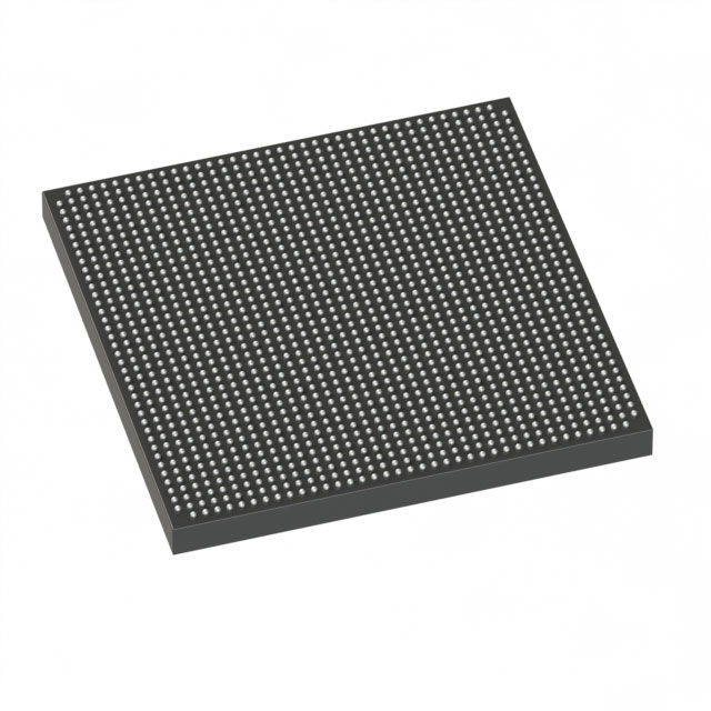
Stratix® V GX Field Programmable Gate Array (FPGA) IC 696 53248000 952000 1517-BBGA, FCBGA |
|---|---|
| Quantity | 425 Available (as of June 15, 2026) |

| Product Category | Field Programmable Gate Array (FPGA) |
|---|---|
| Manufacturer | Intel |
| Manufacturing Status | Obsolete |
| Manufacturer Standard Lead Time | Contact Us |
| Datasheet |
Specifications & Environmental
| Device Package | 1517-HBGA (45x45) | Grade | Commercial | Operating Temperature | 0°C – 85°C | ||
|---|---|---|---|---|---|---|---|
| Package / Case | 1517-BBGA, FCBGA | Number of I/O | 696 | Voltage | 820 mV - 880 mV | ||
| Mounting Method | Surface Mount | RoHS Compliance | RoHS Compliant | REACH Compliance | REACH Unknown | ||
| Moisture Sensitivity Level | 3 (168 Hours) | Number of LABs/CLBs | 359200 | Number of Logic Elements/Cells | 952000 | ||
| Number of Gates | N/A | ECCN | 3A001A2C | HTS Code | 8542.39.0001 | ||
| Qualification | N/A | Total RAM Bits | 53248000 |
Overview of 5SGXMABK2H40C2LN – Stratix® V GX FPGA, 952,000 logic elements, ~53.25 Mbits RAM, 696 I/O
The 5SGXMABK2H40C2LN is an Intel Stratix® V GX field programmable gate array (FPGA) supplied in a 1517-BBGA FCBGA package. It delivers a high-density fabric and substantial on-chip memory for complex logic, signal processing, and high-speed serial interface functions.
Targeted at commercial-grade applications, this device combines 952,000 logic elements, approximately 53.25 Mbits of embedded RAM, and 696 user I/Os to support large FPGA designs that require extensive logic capacity and I/O integration.
Key Features
- High logic density — 952,000 logic elements to implement large-scale digital designs and complex custom accelerators.
- Embedded memory — Approximately 53.25 Mbits of on-chip RAM to support buffering, FIFOs, and intermediate data storage without external memory for many use cases.
- Extensive I/O — 696 user I/Os enabling broad interfacing options for multi-channel systems and dense board-level connectivity.
- Low-voltage core — Core supply specified between 820 mV and 880 mV to align with modern power-optimized FPGA system designs.
- Commercial temperature grade — Rated for 0 °C to 85 °C operation for commercial applications.
- Package and mounting — 1517-BBGA, FCBGA package (supplier device package listed as 1517-HBGA, 45×45 mm) with surface-mount assembly for compact, high-density PCB designs.
- RoHS compliant — Meets environmental compliance requirements for lead-free manufacturing.
Typical Applications
- High-speed communications — Leverage the Stratix V GX family’s transceiver-capable architecture for line-rate packet processing and multi-Gbps serial links.
- Network acceleration — Use the large logic capacity and on-chip RAM for packet inspection, forwarding engines, and custom offload functions.
- Signal processing and compute — Implement complex DSP pipelines and parallel compute engines that require large numbers of logic elements and embedded memory.
- Prototyping and custom SoC integration — Dense I/O and high logic count make this device suitable for prototyping ASIC functions or integrating custom peripherals on an FPGA platform.
Unique Advantages
- Large-scale integration: 952,000 logic elements enable consolidation of multiple functions into a single device, reducing BOM and board complexity.
- Significant embedded RAM: Approximately 53.25 Mbits of on-chip memory supports deep buffering and stateful processing without immediate reliance on external memory.
- High I/O count: 696 I/Os provide flexible interfacing for multi-lane systems, dense peripheral connectivity, and mezzanine-style interconnects.
- Compact package: 1517-BBGA FCBGA in a 45×45 mm supplier package footprint supports high-density board layouts while maintaining surface-mount assembly.
- Commercial readiness: 0 °C to 85 °C operating range and RoHS compliance align the device with mainstream electronics manufacturing and deployment.
- Power-defined core: Specified core voltage range (820 mV–880 mV) allows designers to plan power delivery for optimized efficiency and stability.
Why Choose 5SGXMABK2H40C2LN?
This Stratix V GX FPGA part delivers a balance of very high logic capacity, substantial embedded memory, and a large I/O count in a compact surface-mount BGA package. It is positioned for commercial applications that require consolidation of complex digital functions, high-throughput data handling, and extensive board-level interfacing.
Designers and system architects will find this device suitable when projects demand scalable logic resources, robust on-chip RAM, and flexibility for high-speed serial and parallel interfaces, while aligning with standard commercial temperature and manufacturing requirements.
Request a quote or submit an inquiry to receive pricing, availability, and technical ordering information for the 5SGXMABK2H40C2LN Stratix V GX FPGA.


Date Founded: 1968
Headquarters: Santa Clara, California, USA
Employees: 130,000+
Revenue: $54.23 Billion
Certifications and Memberships: ISO9001:2015, ISO14001:2015, ISO17025:2017, ISO27001:2022, ISO45001:2018, ISO50001:2018


