
5SGXMABK2H40C3N
| Part Description |
Stratix® V GX Field Programmable Gate Array (FPGA) IC 696 53248000 952000 1517-BBGA, FCBGA |
|---|---|
| Quantity | 1,290 Available (as of June 10, 2026) |

| Product Category | Field Programmable Gate Array (FPGA) |
|---|---|
| Manufacturer | Intel |
| Manufacturing Status | Obsolete |
| Manufacturer Standard Lead Time | Contact Us |
| Datasheet |
Specifications & Environmental
| Device Package | 1517-HBGA (45x45) | Grade | Commercial | Operating Temperature | 0°C – 85°C | ||
|---|---|---|---|---|---|---|---|
| Package / Case | 1517-BBGA, FCBGA | Number of I/O | 696 | Voltage | 820 mV - 880 mV | ||
| Mounting Method | Surface Mount | RoHS Compliance | RoHS Compliant | REACH Compliance | REACH Unknown | ||
| Moisture Sensitivity Level | 3 (168 Hours) | Number of LABs/CLBs | 359200 | Number of Logic Elements/Cells | 952000 | ||
| Number of Gates | N/A | ECCN | 3A001A2C | HTS Code | 8542.39.0001 | ||
| Qualification | N/A | Total RAM Bits | 53248000 |
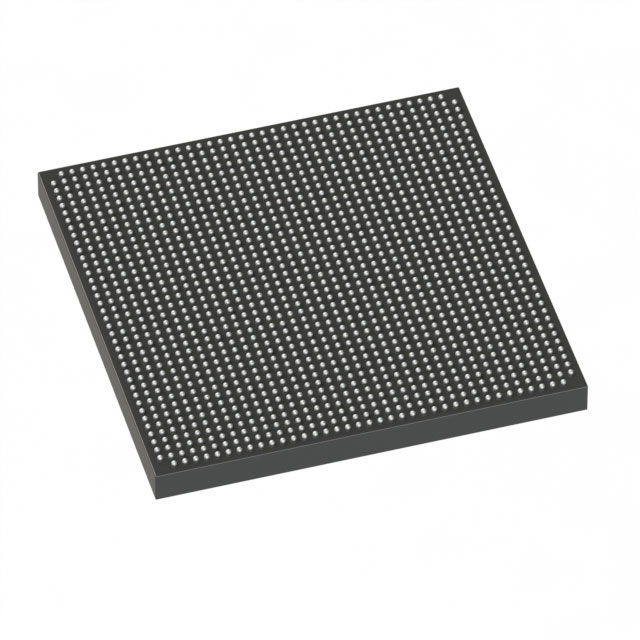
Overview of 5SGXMABK2H40C3N – Stratix® V GX FPGA, 952,000 logic elements, 1517-BBGA
The 5SGXMABK2H40C3N is a Stratix V GX field programmable gate array (FPGA) offered in a 1517-BBGA FCBGA package. This commercial-grade device provides very high logic density and abundant on-chip memory for demanding digital designs.
With 952,000 logic elements, approximately 53.25 Mbits of embedded memory, and 696 I/O pins, the device targets complex data processing, high-density integration, and designs that require extensive programmable logic and I/O resources.
Key Features
- Core Logic Density — 952,000 logic elements provide substantial capacity for large-scale digital designs and complex logic implementation.
- Embedded Memory — Approximately 53.25 Mbits of on-chip RAM for data buffering, large FIFOs, and memory-intensive algorithms.
- I/O Count — 696 I/O pins to support wide data buses, multiple interfaces, and high pin-count board designs.
- Power Supply — Core supply voltage specified at 0.820 V to 0.880 V, enabling defined power delivery planning for the core domain.
- Package & Mounting — 1517-BBGA (FCBGA) package, supplier device package 1517-HBGA (45×45), surface-mount mounting type for compact PCB layouts.
- Operating Range — Commercial temperature grade with an operating range of 0 °C to 85 °C for standard commercial environments.
- RoHS Compliant — Meets RoHS environmental requirements for lead-free assembly.
- Stratix V GX Family Context — As a member of the Stratix V GX family, series documentation describes high-performance transceiver speed grades defined for the family.
Typical Applications
- High-bandwidth data processing — Leverage the large logic capacity and on-chip memory to implement complex pipelines, data aggregation, and parallel processing tasks.
- Networking and communications — The Stratix V GX family defines high-speed transceiver grades; use this device where high I/O counts and series transceiver capabilities are relevant to packet processing and interface bridging.
- Video and imaging systems — Dense logic and substantial embedded RAM support image pipelines, frame buffering, and real-time video processing functions.
- Complex system integration — High I/O density and a compact FCBGA package make the device suitable for consolidating multiple functions into a single FPGA in space-constrained designs.
Unique Advantages
- High integration density: 952,000 logic elements reduce the need for multiple FPGAs, simplifying BOM and board-level interconnect.
- Large embedded memory: Approximately 53.25 Mbits of on-chip RAM enables extensive buffering and state storage without external memory.
- Extensive I/O capability: 696 I/Os support complex interface requirements and wide parallel buses for high-throughput designs.
- Commercial-grade thermal range: Rated 0 °C to 85 °C for reliable operation in standard commercial applications.
- RoHS compliance: Supports lead-free assembly and meets environmental regulations for many markets.
- Compact, production-ready package: 1517-BBGA (FCBGA) with a 45×45 supplier device footprint facilitates high-density PCB integration.
Why Choose 5SGXMABK2H40C3N?
The 5SGXMABK2H40C3N delivers a high-capacity, commercially rated FPGA solution for designs that demand large logic resources, significant on-chip memory, and extensive I/O. Its Stratix V GX family lineage provides access to a platform defined for high-performance transceiver capabilities and series-level electrical characteristics.
This device is suited to system architects and engineers building complex data-paths, video processing pipelines, and multifunction hardware platforms where logic density, memory capacity, and I/O count are primary selection criteria. The combination of package density, defined core supply range, and RoHS compliance offers a clear path to production for commercial applications.
Request a quote or submit an RFQ for 5SGXMABK2H40C3N to obtain pricing, availability, and lead-time information tailored to your project needs.


Date Founded: 1968
Headquarters: Santa Clara, California, USA
Employees: 130,000+
Revenue: $54.23 Billion
Certifications and Memberships: ISO9001:2015, ISO14001:2015, ISO17025:2017, ISO27001:2022, ISO45001:2018, ISO50001:2018


