
5SGXMABK2H40I2LG
| Part Description |
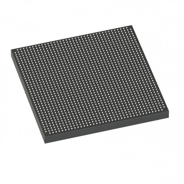
Stratix® V GX Field Programmable Gate Array (FPGA) IC 696 53248000 952000 1517-BBGA, FCBGA |
|---|---|
| Quantity | 661 Available (as of June 15, 2026) |

| Product Category | Field Programmable Gate Array (FPGA) |
|---|---|
| Manufacturer | Intel |
| Manufacturing Status | Active |
| Manufacturer Standard Lead Time | 26 Weeks |
| Datasheet |
Specifications & Environmental
| Device Package | 1517-HBGA (45x45) | Grade | Industrial | Operating Temperature | -40°C – 100°C | ||
|---|---|---|---|---|---|---|---|
| Package / Case | 1517-BBGA, FCBGA | Number of I/O | 696 | Voltage | 820 mV - 880 mV | ||
| Mounting Method | Surface Mount | RoHS Compliance | RoHS Compliant | REACH Compliance | REACH Unaffected | ||
| Moisture Sensitivity Level | 3 (168 Hours) | Number of LABs/CLBs | 359200 | Number of Logic Elements/Cells | 952000 | ||
| Number of Gates | N/A | ECCN | N/A | HTS Code | N/A | ||
| Qualification | N/A | Total RAM Bits | 53248000 |
Overview of 5SGXMABK2H40I2LG – Stratix® V GX FPGA, approximately 952,000 logic elements, 696 I/Os
The 5SGXMABK2H40I2LG is a Stratix V GX field programmable gate array (FPGA) in a 1517‑BBGA FCBGA package, offered in an industrial temperature grade. It provides large on‑chip logic and memory capacity together with high I/O density, intended for designs that require extensive programmable logic, embedded RAM, and high‑speed serial transceiver capabilities as described in the Stratix V device family documentation.
This device targets applications that leverage the Stratix V GX architecture's electrical and switching characteristics, including programmable I/O timing and transceiver functionality defined in the series datasheet.
Key Features
- Logic Capacity — Approximately 952,000 logic elements for large, complex programmable logic implementations.
- Embedded Memory — Approximately 53.25 Mbits of on‑chip RAM for data buffering and state storage.
- I/O Density — 696 user I/Os to support extensive external interfacing and parallel connectivity.
- Transceiver Grade (Series) — Stratix V GX transceiver capabilities are documented in the Stratix V datasheet (series), including supported channel speed grades for high‑speed serial links.
- Power — Core voltage supply specified from 820 mV to 880 mV to match system power delivery requirements.
- Package & Mounting — 1517‑BBGA FCBGA package (supplier device package: 1517‑HBGA, 45×45 mm) optimized for surface‑mount PCB assembly.
- Industrial Temperature Grade — Rated to operate from −40 °C to 100 °C for industrial environments.
- Compliance — RoHS compliant.
Typical Applications
- High‑density logic implementations — Large FPGA designs that require hundreds of thousands of logic elements and substantial on‑chip RAM.
- High‑I/O systems — Designs needing broad parallel connectivity and numerous external interfaces using up to 696 I/Os.
- High‑speed serial links — Systems leveraging Stratix V GX transceiver capabilities for serial communication as specified in the device family datasheet.
- Industrial deployments — Applications requiring an industrial operating range (−40 °C to 100 °C) and RoHS compliance.
Unique Advantages
- Large programmable resource pool: Approximately 952,000 logic elements enable the implementation of complex logic, algorithms, and soft processors without external ASICs.
- Significant on‑chip memory: Approximately 53.25 Mbits of embedded RAM reduces dependence on external memory for many buffering and storage tasks.
- Extensive external interfacing: 696 user I/Os support broad peripheral and parallel bus connectivity to simplify board‑level integration.
- Industrial temperature tolerance: Specified operation from −40 °C to 100 °C for deployment in temperature‑challenging environments.
- Compact, production‑ready package: 1517‑BBGA FCBGA (supplier 1517‑HBGA 45×45) surface‑mount package supports volume assembly and dense PCB layouts.
- Series electrical and switching characterization: Stratix V device datasheet documents operating conditions, switching characteristics, and I/O timing for design validation.
Why Choose 5SGXMABK2H40I2LG?
As a member of the Stratix V GX family, the 5SGXMABK2H40I2LG combines substantial logic capacity, a large pool of embedded RAM, and high I/O density in an industrial‑grade FPGA package. Its specified core voltage range and documented series electrical/switching characteristics make it suitable for complex, high‑resource FPGA designs that need reliable operation across a wide temperature range.
This device is appropriate for engineers and system designers building applications that require dense programmable logic, on‑chip memory, numerous I/Os, and the transceiver capabilities outlined in the Stratix V GX device documentation.
Request a quote or submit an inquiry to receive pricing and availability for 5SGXMABK2H40I2LG and to discuss your design requirements with our team.


Date Founded: 1968
Headquarters: Santa Clara, California, USA
Employees: 130,000+
Revenue: $54.23 Billion
Certifications and Memberships: ISO9001:2015, ISO14001:2015, ISO17025:2017, ISO27001:2022, ISO45001:2018, ISO50001:2018


