
5SGXMB5R1F43C2LN
| Part Description |
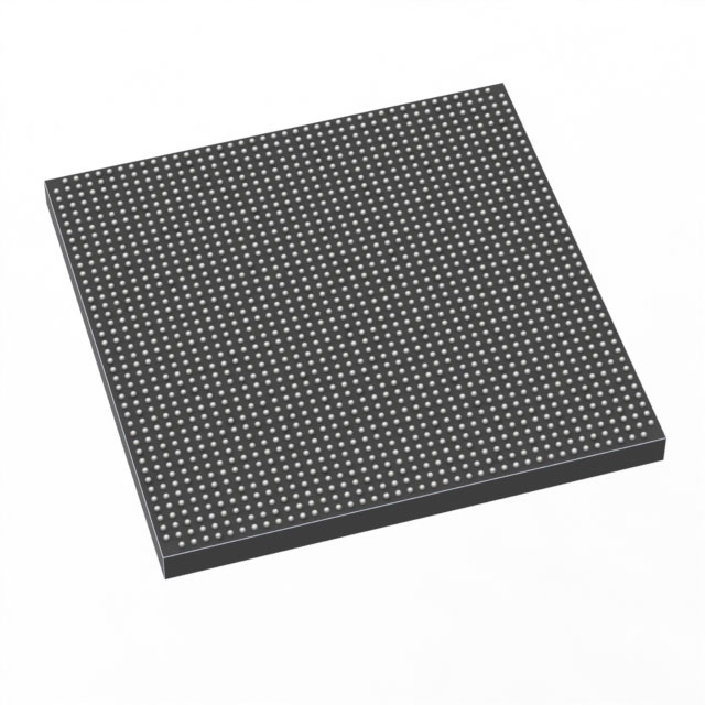
Stratix® V GX Field Programmable Gate Array (FPGA) IC 600 41984000 490000 1760-BBGA, FCBGA |
|---|---|
| Quantity | 787 Available (as of June 16, 2026) |

| Product Category | Field Programmable Gate Array (FPGA) |
|---|---|
| Manufacturer | Intel |
| Manufacturing Status | Obsolete |
| Manufacturer Standard Lead Time | Contact Us |
| Datasheet |
Specifications & Environmental
| Device Package | 1760-FCBGA (42.5x42.5) | Grade | Commercial | Operating Temperature | 0°C – 85°C | ||
|---|---|---|---|---|---|---|---|
| Package / Case | 1760-BBGA, FCBGA | Number of I/O | 600 | Voltage | 820 mV - 880 mV | ||
| Mounting Method | Surface Mount | RoHS Compliance | RoHS Compliant | REACH Compliance | REACH Unknown | ||
| Moisture Sensitivity Level | 3 (168 Hours) | Number of LABs/CLBs | 185000 | Number of Logic Elements/Cells | 490000 | ||
| Number of Gates | N/A | ECCN | 3A001A2C | HTS Code | 8542.39.0001 | ||
| Qualification | N/A | Total RAM Bits | 41984000 |
Overview of 5SGXMB5R1F43C2LN – Stratix® V GX Field Programmable Gate Array, 1760-FCBGA
The 5SGXMB5R1F43C2LN is a Stratix V GX field programmable gate array (FPGA) in a 1760-ball FCBGA/BBGA package. It delivers high logic density and substantial on-chip memory for complex digital designs, with a broad I/O count and support for Stratix V GX transceiver speed grades described in the device family datasheet.
Designed for commercial-grade applications, this device targets designs that require large programmable logic capacity, significant embedded RAM, and high-density connectivity within a 42.5 × 42.5 mm 1760-FCBGA package.
Key Features
- Logic Capacity — 490,000 logic elements to implement large-scale, highly parallel digital designs.
- Embedded Memory — Approximately 42 Mbits of on-chip RAM (41,984,000 bits) for buffers, FIFOs, and local data storage.
- I/O Density — 600 user I/Os to support dense peripheral, bus, and interface routing on complex PCBs.
- Transceiver Speed Grades (Stratix V GX family) — Stratix V GX devices include transceiver speed grades listed in the datasheet (examples include GX channel—14.1 Gbps and 12.5 Gbps), providing options for high-speed serial interfaces at the family level.
- Power and Voltage — Core supply operating range of 820 mV to 880 mV for core power planning and thermal design.
- Package — 1760-FCBGA / 1760-BBGA package, supplier device package specified as 1760-FCBGA (42.5 × 42.5 mm), suitable for high-density board layouts.
- Commercial Grade Temperature — Rated for operation from 0 °C to 85 °C, meeting commercial temperature requirements.
- Environmental Compliance — RoHS compliant.
Typical Applications
- High-speed serial interfaces — Use the Stratix V GX family transceiver speed grades to implement high-bandwidth serial links where supported by the device family.
- Compute- and signal-processing designs — Large logic element count and substantial embedded RAM support complex processing pipelines and parallel algorithms.
- Dense I/O systems — With 600 I/Os, integrate multiple peripherals, memory interfaces, or board-level buses in a single FPGA.
- Complex system integration — High logic capacity and package density enable consolidation of multiple functions into one programmable device for advanced commercial systems.
Unique Advantages
- High logic integration: 490,000 logic elements reduce the need for multiple devices by accommodating large designs in one FPGA.
- Significant on-chip memory: Approximately 42 Mbits of embedded RAM simplifies data buffering and on-chip storage for memory-intensive functions.
- Extensive I/O: 600 I/Os provide flexibility for routing multiple external interfaces without external multiplexing.
- Family-level transceiver options: Stratix V GX family transceiver speed grades (as documented in the datasheet) support a range of high-speed serial link requirements at the family level.
- Compact, high-density package: 1760-FCBGA (42.5 × 42.5 mm) enables high-density PCB designs while keeping the solution integrated.
- Commercial operating range: Rated 0 °C to 85 °C for deployment in commercial-grade systems.
Why Choose 5SGXMB5R1F43C2LN?
The 5SGXMB5R1F43C2LN combines substantial logic capacity, large on-chip memory, and a high I/O count in a single commercial-grade Stratix V GX FPGA package. It is well suited for designers who need to implement complex, high-density logic and memory architectures while retaining options for high-speed serial interfaces at the Stratix V GX family level.
For teams developing advanced commercial systems, this device offers a balance of performance, integration, and environmental compliance that supports scalable, long-lived designs backed by the Stratix V device family documentation.
Request a quote or submit an inquiry for 5SGXMB5R1F43C2LN to receive pricing and availability information tailored to your project needs.


Date Founded: 1968
Headquarters: Santa Clara, California, USA
Employees: 130,000+
Revenue: $54.23 Billion
Certifications and Memberships: ISO9001:2015, ISO14001:2015, ISO17025:2017, ISO27001:2022, ISO45001:2018, ISO50001:2018


