
5SGXMB5R1F43I2N
| Part Description |
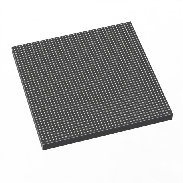
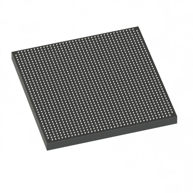
Stratix® V GX Field Programmable Gate Array (FPGA) IC 600 41984000 490000 1760-BBGA, FCBGA |
|---|---|
| Quantity | 712 Available (as of June 15, 2026) |

| Product Category | Field Programmable Gate Array (FPGA) |
|---|---|
| Manufacturer | Intel |
| Manufacturing Status | Obsolete |
| Manufacturer Standard Lead Time | Contact Us |
| Datasheet |
Specifications & Environmental
| Device Package | 1760-FCBGA (42.5x42.5) | Grade | Industrial | Operating Temperature | -40°C – 100°C | ||
|---|---|---|---|---|---|---|---|
| Package / Case | 1760-BBGA, FCBGA | Number of I/O | 600 | Voltage | 870 mV - 930 mV | ||
| Mounting Method | Surface Mount | RoHS Compliance | RoHS Compliant | REACH Compliance | REACH Unknown | ||
| Moisture Sensitivity Level | 3 (168 Hours) | Number of LABs/CLBs | 185000 | Number of Logic Elements/Cells | 490000 | ||
| Number of Gates | N/A | ECCN | 3A001A2C | HTS Code | 8542.39.0001 | ||
| Qualification | N/A | Total RAM Bits | 41984000 |
Overview of 5SGXMB5R1F43I2N – Stratix® V GX FPGA, 1760‑FCBGA (42.5×42.5), Industrial
The 5SGXMB5R1F43I2N is an Intel Stratix V GX field‑programmable gate array in a 1760‑ball FCBGA package. It delivers very large logic capacity and embedded memory with extensive I/O while operating across an industrial temperature range, making it suitable for demanding, high‑density FPGA designs.
Built on the Stratix V GX family architecture, the device targets applications requiring high logic count, abundant on‑chip RAM, and multi‑gigabit serial connectivity options provided by the GX transceiver family described in the device series datasheet.
Key Features
- Logic Capacity — 490,000 logic elements to implement complex digital designs and large system functions on a single device.
- Embedded Memory — Approximately 42 Mbits of embedded RAM bits for buffering, FIFOs, and on‑chip storage.
- I/O Density — 600 I/O pins to support dense board connectivity, parallel interfaces, and multiple high‑speed PHYs.
- High‑Speed Transceiver Family — Part of the Stratix V GX family; the series datasheet documents GX transceiver speed grades used for multi‑gigabit serial links.
- Power and Supply — Core voltage supply range of 870 mV to 930 mV for core power planning and regulator selection.
- Package and Mounting — 1760‑FCBGA (42.5 × 42.5 mm) surface‑mount package for high‑pin‑count boards and compact system integration.
- Industrial Temperature Grade — Rated for operation from −40 °C to 100 °C for deployment in industrial environments.
- RoHS Compliant — Meets RoHS environmental requirements for regulated materials.
Typical Applications
- High‑speed communications — Use the Stratix V GX transceiver family capabilities and 600 I/Os to implement multi‑gigabit links, PHY aggregation, and protocol bridging.
- Network and data‑plane acceleration — Large logic capacity and abundant on‑chip RAM enable packet processing, flow classification, and hardware acceleration functions.
- Video and signal processing — High logic density and memory resources support complex DSP pipelines, frame buffering, and real‑time processing.
- Test & measurement and instrumentation — Industrial temperature rating and wide I/O complement demanding, rack‑mounted or field test equipment designs.
Unique Advantages
- High integration density: 490,000 logic elements and ~42 Mbits of embedded RAM reduce the need for external logic and memory, simplifying system design.
- Extensive I/O support: 600 I/Os provide flexibility for interfacing to numerous peripherals, parallel buses, and multiple serial lanes on the same device.
- Industrial robustness: Specified for −40 °C to 100 °C operation to meet the thermal demands of industrial deployments.
- Compact, high‑pin package: 1760‑FCBGA (42.5×42.5 mm) enables dense board layouts while maintaining signal routing capacity for complex systems.
- Controlled core supply range: 870–930 mV core voltage specification supports predictable power budgeting and regulator selection.
- Environmentally compliant: RoHS compliance simplifies regulatory compliance for end products.
Why Choose 5SGXMB5R1F43I2N?
The 5SGXMB5R1F43I2N combines very large logic and memory resources with high I/O counts and the Stratix V GX transceiver family characteristics, making it well suited to high‑bandwidth, compute‑intensive FPGA implementations in industrial settings. Its FCBGA package enables dense system integration while the specified core voltage and temperature range support predictable power and thermal planning.
This device is appropriate for engineering teams building scalable, high‑performance systems that require on‑chip capacity for complex algorithms, multi‑lane serial interfaces, and extensive external connectivity, backed by the Stratix V device family documentation and specifications.
Request a quote or submit a technical inquiry to obtain pricing, availability, and delivery details for part number 5SGXMB5R1F43I2N.


Date Founded: 1968
Headquarters: Santa Clara, California, USA
Employees: 130,000+
Revenue: $54.23 Billion
Certifications and Memberships: ISO9001:2015, ISO14001:2015, ISO17025:2017, ISO27001:2022, ISO45001:2018, ISO50001:2018


