
A3PN015-2QNG68
| Part Description |
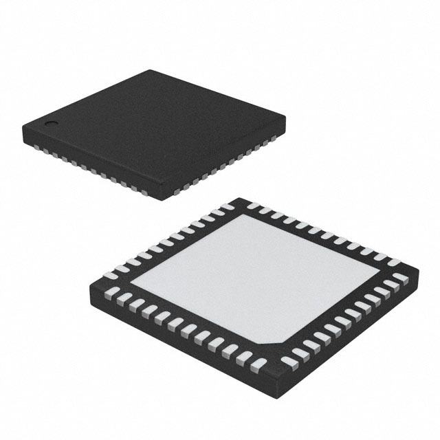
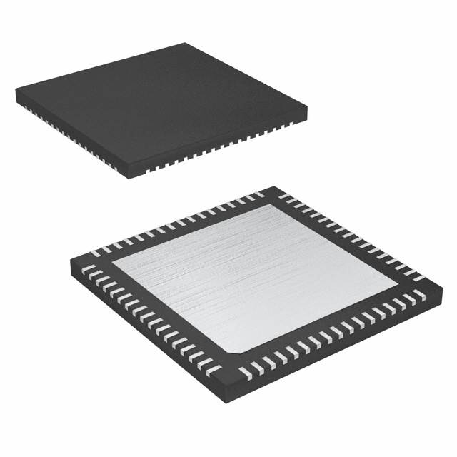
ProASIC3 nano Field Programmable Gate Array (FPGA) IC 49 68-VFQFN Exposed Pad |
|---|---|
| Quantity | 958 Available (as of June 15, 2026) |

| Product Category | Field Programmable Gate Array (FPGA) |
|---|---|
| Manufacturer | Microchip Technology |
| Manufacturing Status | Active |
| Manufacturer Standard Lead Time | 8 Weeks |
| Datasheet |
Specifications & Environmental
| Device Package | 68-QFN (8x8) | Grade | Commercial | Operating Temperature | -20°C – 85°C | ||
|---|---|---|---|---|---|---|---|
| Package / Case | 68-VFQFN Exposed Pad | Number of I/O | 49 | Voltage | 1.425 V - 1.575 V | ||
| Mounting Method | Surface Mount | RoHS Compliance | ROHS3 Compliant | REACH Compliance | REACH Unaffected | ||
| Moisture Sensitivity Level | 3 (168 Hours) | Number of LABs/CLBs | 384 | Number of Logic Elements/Cells | 384 | ||
| Number of Gates | 15000 | ECCN | 3A991D | HTS Code | 8542.39.0001 | ||
| Qualification | N/A |
Overview of A3PN015-2QNG68 – ProASIC3 nano Field Programmable Gate Array (FPGA) IC 49 68-VFQFN Exposed Pad
The A3PN015-2QNG68 is a ProASIC3 nano FPGA device offering a compact, surface-mount 68-VFQFN package with an exposed pad. It provides a low-voltage programmable logic solution with 384 logic elements and 49 I/O pins for commercial-grade embedded designs.
Intended for applications that require moderate gate density and flexible I/O in a small footprint, this device delivers a balance of integration and power efficiency through a narrow 1.425 V to 1.575 V supply window and an operating temperature range of -20 °C to 85 °C.
Key Features
- Logic Capacity Approximately 384 logic elements and 15,000 gates for implementing glue logic, control state machines, and small custom digital functions.
- I/O Count 49 general-purpose I/O pins suitable for sensor interfaces, peripheral control, and protocol bridging in compact systems.
- Power Designed for low-voltage systems with a supply range of 1.425 V to 1.575 V to match tight power-rail requirements.
- Package and Mounting 68-VFQFN package with exposed pad in a 68-QFN (8×8) supplier package footprint; surface-mount for dense PCB layouts and improved thermal contact.
- Temperature Grade Commercial operating range from -20 °C to 85 °C for standard electronics and consumer applications.
- Compliance RoHS-compliant design to meet common environmental and assembly requirements.
- Memory Architecture This device is focused on logic and I/O capability (Total on‑chip RAM: 0 bits), providing deterministic resources for dedicated combinational and sequential logic tasks.
Typical Applications
- Embedded Control Implement compact control logic and state machines for consumer and commercial products where a small programmable device is required.
- Protocol Bridging Provide I/O buffering and simple protocol translation between peripherals and system controllers using available GPIO resources.
- User Interface Control Drive and manage buttons, LEDs, and simple displays while offloading repetitive tasks from the main MCU.
- Sensor Interfacing Aggregate and condition digital sensor signals with programmable logic and moderate I/O counts in space-constrained designs.
Unique Advantages
- Space-efficient package: The 68-VFQFN (8×8) exposed-pad footprint minimizes PCB area while supporting thermal dissipation through the pad.
- Right-sized logic density: Approximately 384 logic elements and 15,000 gates provide the capacity needed for glue logic and compact digital functions without excess overhead.
- Low-voltage compatibility: Tight supply range (1.425 V–1.575 V) aligns the device with modern low-voltage platforms and power domains.
- Commercial temperature suitability: Rated for -20 °C to 85 °C, matching common temperature requirements for business and consumer electronics.
- RoHS compliant: Ready for lead-free assembly flows and environmental compliance requirements.
Why Choose A3PN015-2QNG68?
The A3PN015-2QNG68 positions itself as a practical, compact FPGA option for commercial applications that need programmable logic and flexible I/O in a small, surface-mount package. Its combination of approximately 384 logic elements, 49 I/Os, and a low-voltage supply range makes it well suited for designers looking to implement deterministic digital functions, protocol adaptation, or control logic without a large form factor or high resource overhead.
For teams focused on reducing BOM complexity and optimizing PCB space, this device delivers a focused feature set backed by RoHS compliance and a package designed for effective thermal conduction via the exposed pad.
Request a quote or submit an inquiry to receive pricing, availability, and support information for the A3PN015-2QNG68.


Date Founded: 1989
Headquarters: Chandler, Arizona, USA
Employees: 22,000+
Revenue: $8.349 Billion
Certifications and Memberships: ISO9001:2015, IATF16949:2016, AS 9100D


