
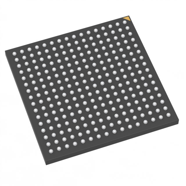
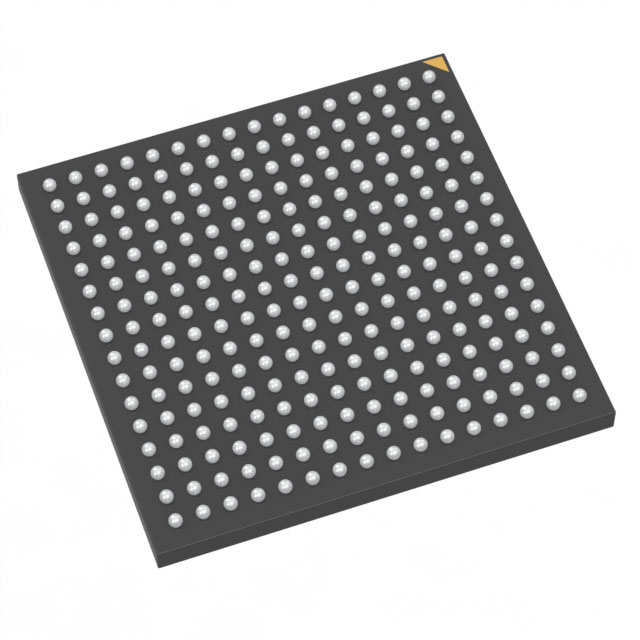
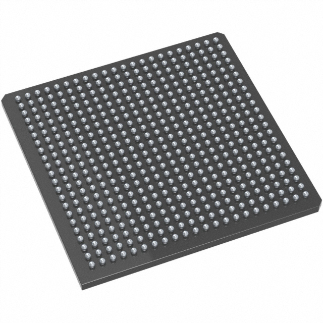
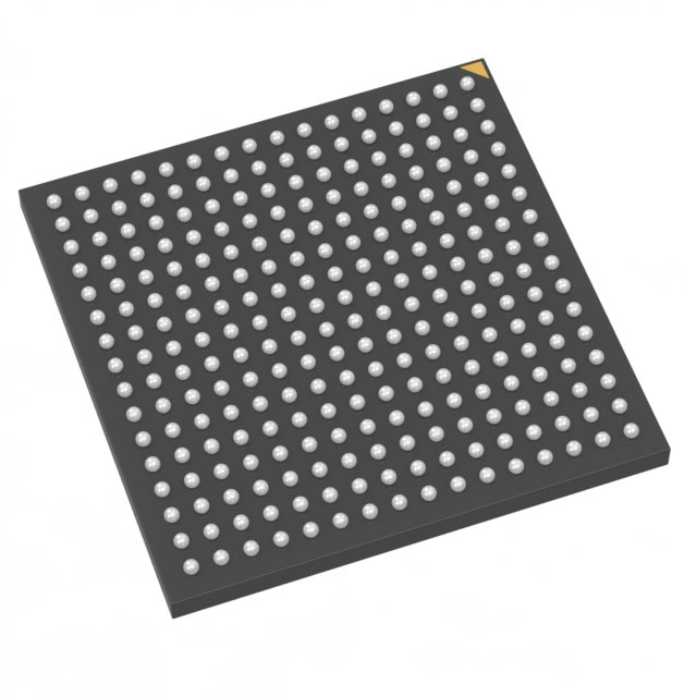
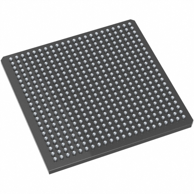
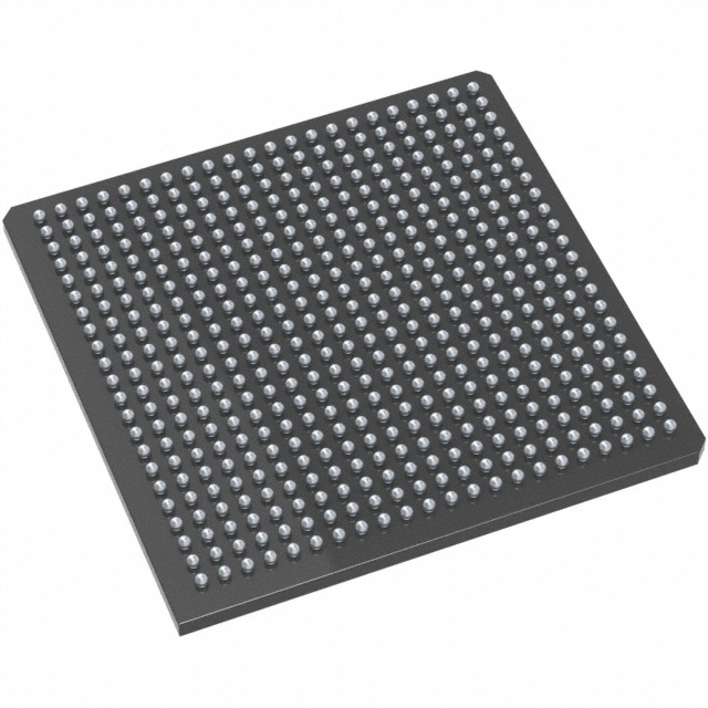
AFS1500-FG256
| Part Description |
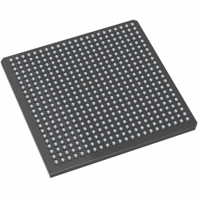
Fusion® Field Programmable Gate Array (FPGA) IC 119 276480 256-LBGA |
|---|---|
| Quantity | 324 Available (as of October 7, 2026) |
| Product Category | Field Programmable Gate Array (FPGA) |
|---|---|
| Manufacturer | Microchip Technology |
| Manufacturing Status | Active |
| Manufacturer Standard Lead Time | 16 Weeks |
| Datasheet |
Specifications & Environmental
| Device Package | 256-FPBGA (17x17) | Grade | Commercial | Operating Temperature | 0°C – 85°C | ||
|---|---|---|---|---|---|---|---|
| Package / Case | 256-LBGA | Number of I/O | 119 | Voltage | 1.425 V - 1.575 V | ||
| Mounting Method | Surface Mount | RoHS Compliance | RoHS non-compliant | REACH Compliance | REACH Unaffected | ||
| Moisture Sensitivity Level | 3 (168 Hours) | Number of LABs/CLBs | 38400 | Number of Logic Elements/Cells | 38400 | ||
| Number of Gates | 1500000 | ECCN | 3A991D | HTS Code | 8542.39.0001 | ||
| Qualification | N/A | Total RAM Bits | 276480 |
Overview of AFS1500-FG256 – Fusion® Field Programmable Gate Array (FPGA) IC, 119 I/Os, ~276480-bit RAM, 256-LBGA
The AFS1500-FG256 is a Fusion® Field Programmable Gate Array (FPGA) IC offering a balanced mix of programmable logic, on-chip memory, and I/O capacity in a compact 256-LBGA package. With 38,400 logic elements and approximately 276,480 bits of embedded memory, this commercial-grade FPGA is suited for tasks that require customizable digital logic, moderate embedded memory, and substantial I/O connectivity.
Designed for surface-mount assembly and RoHS compliance, the AFS1500-FG256 supports designs that operate within a 1.425 V to 1.575 V supply range and a 0 °C to 85 °C operating temperature window.
Key Features
- Core Logic 38,400 logic elements delivering programmable resources equivalent to 1,500,000 gates for implementing custom digital functions and complex combinational/sequential logic.
- Embedded Memory Approximately 0.276 Mbits (276,480 bits) of on-chip RAM for local data buffering, FIFOs, and small lookup tables without external memory.
- I/O Capacity 119 general-purpose I/O pins to support multiple interface signals, parallel buses, and I/O-rich designs.
- Package and Mounting 256-LBGA package (supplier device package: 256-FPBGA, 17×17) optimized for surface-mount assembly and dense board layouts.
- Power Operates from a 1.425 V to 1.575 V supply range, allowing designers to plan power rails precisely for stable operation.
- Operating Conditions Commercial grade operation from 0 °C to 85 °C for standard environment applications.
- Regulatory RoHS compliant to support lead-free manufacturing and environmental requirements.
Typical Applications
- Custom Digital Logic — Implement state machines, protocol handlers, and bespoke processing blocks using the device's 38,400 logic elements and 1,500,000-gate equivalence.
- I/O Bridging and Bus Interfaces — Use the 119 I/Os to interface between multiple digital peripherals, sensors, and external buses in compact systems.
- Embedded Control and Signal Processing — Leverage on-chip RAM for buffering and small-scale data processing tasks in control and signal path applications.
- Prototyping and Low- to Medium-Volume Systems — Surface-mount 256-LBGA package and commercial temperature rating make it suitable for development boards and production runs within standard environmental ranges.
Unique Advantages
- Substantial Logic Density: 38,400 logic elements (approx. 1,500,000 gates) provide the capacity to implement complex digital designs without discrete ASIC costs.
- On-Chip Memory: Approximately 0.276 Mbits of embedded RAM reduces dependence on external memory for small buffers and lookup tables.
- Ample I/O Count: 119 I/Os enable flexible connectivity for multi-sensor systems, parallel interfaces, and bus bridging.
- Compact, Assembly-Friendly Package: 256-LBGA (256-FPBGA, 17×17) supports dense PCB integration and surface-mount manufacturing processes.
- Predictable Power Requirements: Narrow supply window (1.425 V–1.575 V) assists in targeted power-supply design and board-level power budgeting.
- RoHS Compliant: Facilitates lead-free assembly and simplifies compliance with environmental manufacturing requirements.
Why Choose AFS1500-FG256?
The AFS1500-FG256 combines a sizable logic fabric, embedded RAM, and a high I/O count in a compact 256-LBGA package, offering a practical balance of integration and flexibility for commercial applications. Its defined supply range and commercial operating temperature make it suitable for designers who require predictable electrical and thermal characteristics while implementing custom digital functions.
This device is a good fit for engineers and teams building mid-complexity FPGA-based solutions that need programmable logic density, moderate on-chip memory, and extensive I/O without moving to larger form-factor devices.
Request a quote or submit an inquiry today to discuss pricing, lead times, and how the AFS1500-FG256 can be integrated into your next design.





















Date Founded: 1989
Headquarters: Chandler, Arizona, USA
Employees: 22,000+
Revenue: $8.349 Billion
Certifications and Memberships: ISO9001:2015, IATF16949:2016, AS 9100D




