
AGLP125V2-CS289I
| Part Description |
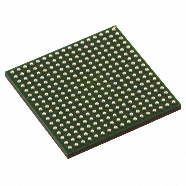
IGLOO PLUS Field Programmable Gate Array (FPGA) IC 212 36864 3120 289-TFBGA, CSBGA |
|---|---|
| Quantity | 537 Available (as of June 18, 2026) |
| Product Category | Field Programmable Gate Array (FPGA) |
|---|---|
| Manufacturer | Microchip Technology |
| Manufacturing Status | Obsolete |
| Manufacturer Standard Lead Time | Contact Us |
| Datasheet |
Specifications & Environmental
| Device Package | 289-CSP (14x14) | Grade | Industrial | Operating Temperature | -40°C – 100°C | ||
|---|---|---|---|---|---|---|---|
| Package / Case | 289-TFBGA, CSBGA | Number of I/O | 212 | Voltage | 1.14 V - 1.575 V | ||
| Mounting Method | Surface Mount | RoHS Compliance | RoHS non-compliant | REACH Compliance | REACH Unaffected | ||
| Moisture Sensitivity Level | 3 (168 Hours) | Number of LABs/CLBs | 3120 | Number of Logic Elements/Cells | 3120 | ||
| Number of Gates | 125000 | ECCN | 3A991D | HTS Code | 8542.39.0001 | ||
| Qualification | N/A | Total RAM Bits | 36864 |
Overview of AGLP125V2-CS289I – IGLOO PLUS FPGA, 125k Gates, 212 I/Os, 289-TFBGA
The AGLP125V2-CS289I is a Microchip Technology IGLOO PLUS flash-based Field Programmable Gate Array (FPGA) offered in a 289-TFBGA (289-CSP, 14×14) surface-mount package. Built on a 130 nm flash process, this device provides reprogrammable nonvolatile configuration, clock conditioning with an integrated PLL, and mixed-voltage I/O support for flexible system integration.
Targeted at designs that require low power, on-chip embedded memory, and a compact package, the AGLP125V2-CS289I is suitable for industrial applications requiring up to 125,000 system gates, approximately 36 kbits of embedded SRAM, and up to 212 user I/Os, while operating across an industrial temperature range.
Key Features
- Logic Capacity — 125,000 system gates and 3,120 logic elements provide ample combinational and sequential resources for medium-density FPGA designs.
- Embedded Memory — Approximately 36 kbits (36,864 bits) of true dual-port SRAM and 1 kbit of on-chip FlashROM for user nonvolatile storage and buffering.
- I/O and Voltage — Up to 212 user I/Os with bank-selectable mixed-voltage operation (1.2 V, 1.5 V, 1.8 V, 2.5 V, 3.3 V) and support for wide-range I/O supply voltages per JESD8 ranges.
- Power and Low-Power Modes — Flash*Freeze technology for ultra-low power retention of configuration and I/O states; typical Flash*Freeze mode for the AGLP125 family member is approximately 16 μW. Core supply support and device supply range includes 1.14 V to 1.575 V.
- Clocking and PLL — Integrated clock conditioning circuitry with six CCC blocks and one integrated PLL for frequency synthesis, phase shift, and clock deskewing.
- Security and In-System Programming — On-chip 128-bit AES decryption for secure in-system programming (ISP) and FlashLock® functionality to protect FPGA contents.
- Package and Mounting — 289-TFBGA (supplier device package 289-CSP 14×14) surface-mount package suitable for compact PCB layouts.
- Industrial Temperature Range — Rated for operation from −40 °C to 100 °C for industrial deployments.
- Standards and Test — JTAG (IEEE 1149.1) boundary-scan support for board-level testability.
- Compliance — RoHS compliant.
Typical Applications
- Industrial Control — Implements control logic, real-time interfacing, and sensor aggregation in industrial systems using the device’s I/O density and industrial temperature rating.
- Power and System Management — Leverages Flash*Freeze and Low Power Active modes to enable low-power monitoring and system power sequencing while preserving configuration and I/O states.
- Secure Embedded Systems — Uses on-chip AES ISP and FlashLock to secure firmware and configuration during in-system programming and deployment.
- Human-Machine Interfaces and Peripheral Control — Supports user-interface scanning and peripheral control with abundant I/Os and low-power standby behavior described in Flash*Freeze use cases.
Unique Advantages
- Nonvolatile, Reprogrammable Flash — Retains programmed design when powered off while allowing field reprogramming for design updates and iterations.
- Low Standby Power with Retention — Flash*Freeze provides ultra-low power retention of design state and I/O, enabling energy-efficient system-level power strategies.
- Integrated Clock Conditioning — Multiple CCC blocks and an integrated PLL simplify clock distribution and frequency management without external clock-conditioning components.
- Flexible Mixed-Voltage I/O — Bank-selectable I/O voltages and wide I/O supply ranges allow direct interfacing to a variety of system logic levels and legacy peripherals.
- Compact, Surface-Mount Package — 289-TFBGA (14×14 CSP) packaging minimizes board area while delivering up to 212 user I/Os for dense designs.
- Industrial Grade Reliability — Rated for −40 °C to 100 °C operation, suitable for demanding environmental conditions.
Why Choose AGLP125V2-CS289I?
The AGLP125V2-CS289I combines Microchip’s IGLOO PLUS flash FPGA architecture with a compact 289-TFBGA package to deliver a reprogrammable, nonvolatile logic fabric with significant I/O and embedded memory for medium-density designs. Its integrated PLL/clock conditioning, secure ISP features, and mixed-voltage I/O support make it a practical choice for industrial control, power management, and secure embedded applications that need instant-on behavior and field reprogrammability.
Designed for engineers who need a balance of logic capacity, low-power modes, and secure in-system update capabilities, this device offers a reliable platform for products that must operate across an industrial temperature range while minimizing external BOM for clocking and nonvolatile storage.
Request a quote or submit a request for pricing and availability to evaluate the AGLP125V2-CS289I for your next design.


Date Founded: 1989
Headquarters: Chandler, Arizona, USA
Employees: 22,000+
Revenue: $8.349 Billion
Certifications and Memberships: ISO9001:2015, IATF16949:2016, AS 9100D


