
AGLP125V2-CSG281
| Part Description |
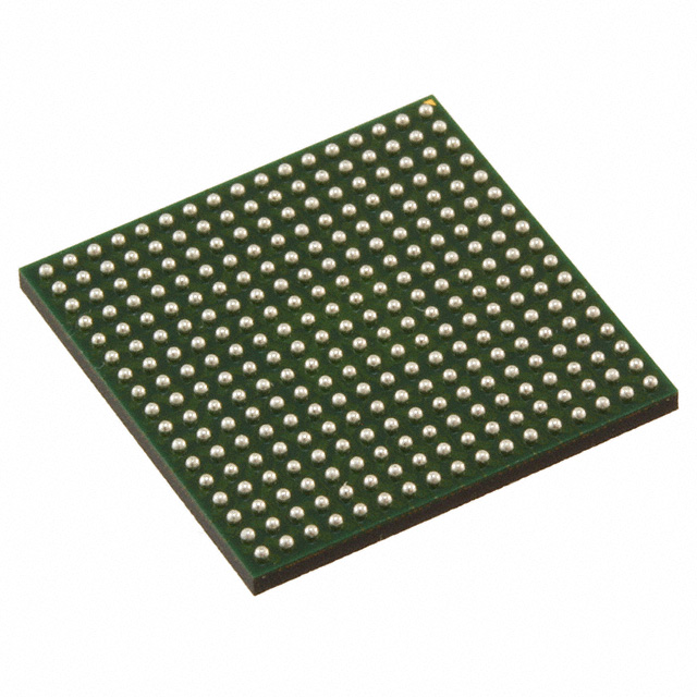
IGLOO PLUS Field Programmable Gate Array (FPGA) IC 212 36864 3120 281-TFBGA, CSBGA |
|---|---|
| Quantity | 1,674 Available (as of October 8, 2026) |

| Product Category | Field Programmable Gate Array (FPGA) |
|---|---|
| Manufacturer | Microchip Technology |
| Manufacturing Status | Obsolete |
| Manufacturer Standard Lead Time | Contact Us |
| Datasheet |
Specifications & Environmental
| Device Package | 281-CSP (10x10) | Grade | Commercial | Operating Temperature | 0°C – 85°C | ||
|---|---|---|---|---|---|---|---|
| Package / Case | 281-TFBGA, CSBGA | Number of I/O | 212 | Voltage | 1.14 V - 1.575 V | ||
| Mounting Method | Surface Mount | RoHS Compliance | RoHS Compliant | REACH Compliance | REACH Unaffected | ||
| Moisture Sensitivity Level | 3 (168 Hours) | Number of LABs/CLBs | 3120 | Number of Logic Elements/Cells | 3120 | ||
| Number of Gates | 125000 | ECCN | 3A991D | HTS Code | 8542.39.0001 | ||
| Qualification | N/A | Total RAM Bits | 36864 |
Overview of AGLP125V2-CSG281 – IGLOO PLUS Flash FPGA, 3,120 Logic Elements, 36 kbits RAM, 212 I/Os, 281-TFBGA
The AGLP125V2-CSG281 is an IGLOO PLUS flash FPGA from Microchip Technology, built on a 130 nm flash CMOS process. It delivers a low-power, single-chip programmable solution with reprogrammable FlashROM, on-chip SRAM, and an advanced I/O mix for compact, power-conscious embedded designs.
With 125,000 system gates, approximately 36 kbits of embedded memory, and up to 212 user I/Os in a 281-TFBGA/CSBGA package, this device targets applications that need small footprint, low standby power and flexible I/O voltage support while operating in commercial temperature ranges.
Key Features
- Core and Logic: 125,000 system gates with 3,120 logic elements provided for combinational and sequential logic implementation.
- Memory & Storage: Approximately 36 kbits of on-chip SRAM and 1 kbit of reprogrammable FlashROM for configuration and small nonvolatile storage.
- Low-Power Operation: Flash*Freeze ultra-low power mode and Low Power Active capability enable micro-watt standby behavior and low-power active control of system functions.
- I/O Flexibility: Up to 212 user I/Os with mixed-voltage support and bank-selectable I/O voltages for interfacing across multiple supply domains.
- Security & In-System Programming: Reprogrammable flash architecture with support for secure, in-system programming and on-chip protections.
- Package & Mounting: Surface-mount 281-TFBGA, CSBGA package; supplier device package listed as 281-CSP (10×10) for compact board-level integration.
- Power and Temperature: Supported supply range 1.14 V to 1.575 V and rated for commercial operating temperatures from 0 °C to 85 °C.
- Compliance: RoHS compliant for lead-free assembly processes.
Typical Applications
- Battery-powered and portable equipment: Flash*Freeze and low-power active modes enable very low standby consumption, extending battery life in portable systems.
- Secure embedded systems: On-chip FlashROM with secure in-system programming capabilities supports instant-on, protected designs.
- Interface and I/O expansion: Up to 212 mixed-voltage I/Os allow the FPGA to act as an I/O bridge, protocol adapter, or control interface in space-constrained boards.
- Compact consumer electronics: Small 281-CSP package and single-chip reprogrammable logic simplify BOM and reduce PCB area for compact product designs.
Unique Advantages
- Ultra-low standby power: Flash*Freeze technology enables micro-watt power retention of configuration, registers and I/O states for long battery life and low quiescent consumption.
- Nonvolatile, reprogrammable Flash: Single-chip flash-based FPGA retains design when powered off and supports in-system reprogramming for field updates.
- High I/O density in a small package: Up to 212 user I/Os in a compact 281-TFBGA footprint helps reduce board area while providing extensive external connectivity.
- Flexible I/O voltage support: Mixed-voltage I/O and bank-selectable voltages simplify interfacing to multiple logic families and peripherals.
- Commercial-temperature qualification: Rated for 0 °C to 85 °C operation to match mainstream consumer and commercial embedded designs.
- RoHS compliant: Compliant with lead-free manufacturing requirements for modern assembly processes.
Why Choose AGLP125V2-CSG281?
The AGLP125V2-CSG281 combines a high gate count and substantial I/O capacity with low-power flash technology to deliver a compact, reprogrammable FPGA platform suited for commercial embedded systems. Its blend of nonvolatile configuration, secure in-system programming, and very low-power standby modes makes it a practical choice where instant-on behavior and long idle periods are required.
This device is ideal for designers seeking a single-chip, small-footprint FPGA that balances logic density, embedded memory, and flexible I/O voltages for consumer and commercial applications. The commercial temperature rating and RoHS compliance support standard production and assembly flows while reducing BOM complexity compared with multi-chip alternatives.
Request a quote or submit a pricing inquiry to receive availability and lead-time information for the AGLP125V2-CSG281.




















Date Founded: 1989
Headquarters: Chandler, Arizona, USA
Employees: 22,000+
Revenue: $8.349 Billion
Certifications and Memberships: ISO9001:2015, IATF16949:2016, AS 9100D




