
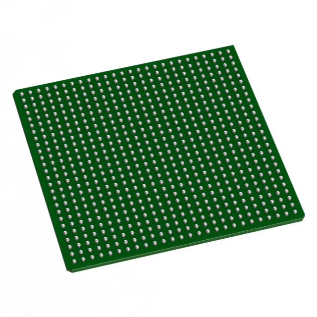
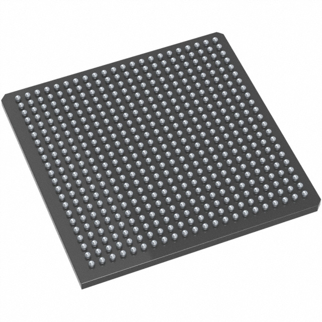
AX1000-2FG676
| Part Description |
Axcelerator Field Programmable Gate Array (FPGA) IC 418 165888 676-BGA |
|---|---|
| Quantity | 65 Available (as of June 10, 2026) |

| Product Category | Field Programmable Gate Array (FPGA) |
|---|---|
| Manufacturer | Microchip Technology |
| Manufacturing Status | Active |
| Manufacturer Standard Lead Time | 12 Weeks |
| Datasheet |
Specifications & Environmental
| Device Package | 676-FBGA (27x27) | Grade | Commercial | Operating Temperature | 0°C – 70°C | ||
|---|---|---|---|---|---|---|---|
| Package / Case | 676-BGA | Number of I/O | 418 | Voltage | 1.425 V - 1.575 V | ||
| Mounting Method | Surface Mount | RoHS Compliance | RoHS non-compliant | REACH Compliance | REACH Unaffected | ||
| Moisture Sensitivity Level | 3 (168 Hours) | Number of LABs/CLBs | 18144 | Number of Logic Elements/Cells | 18144 | ||
| Number of Gates | 1000000 | ECCN | 3A001A7A | HTS Code | 8542.39.0001 | ||
| Qualification | N/A | Total RAM Bits | 165888 |
Overview of AX1000-2FG676 – Axcelerator FPGA IC, 676-FBGA (27×27), 418 I/Os
The AX1000-2FG676 is an Axcelerator family Field Programmable Gate Array (FPGA) from Microchip Technology based on the AX architecture and antifuse programming technology. It delivers a single-chip, nonvolatile FPGA solution with a high gate count and extensive I/O capability for designs that require on-chip memory, deterministic timing and flexible I/O standards.
This device targets applications requiring high-performance programmable logic, high-density I/O and embedded memory with on-chip FIFO control logic, while operating from a 1.425 V to 1.575 V supply and a commercial temperature range of 0 °C to 70 °C.
Key Features
- Core Capacity: 1,000,000 equivalent system gates and 18,144 logic elements provide substantial logic density for complex designs.
- Embedded Memory & FIFO: Total on-chip RAM of 165,888 bits (approximately 0.166 Mbits) with embedded FIFO control logic and variable-aspect RAM blocks available in the Axcelerator family.
- I/O Density & Standards: 418 user I/Os supporting multi-standard operation including single-ended and differential interfaces; LVDS-capable I/Os up to 700 Mb/s are supported in the Axcelerator family.
- High Performance: Family-level performance characteristics include 350+ MHz system performance and 500+ MHz internal performance, plus embedded PLLs with frequency synthesis capabilities up to 1 GHz.
- Security & Nonvolatile Programming: Antifuse-based single-chip nonvolatile programming and FuseLock™ programming technology to protect design IP against reverse engineering.
- Packaging & Mounting: 676-FBGA (27×27) package in a surface-mount form factor, suitable for high-density board layouts.
- Power & Temperature: Core supply range of 1.425 V to 1.575 V; listed commercial operating temperature range of 0 °C to 70 °C and a nominal 1.5 V core voltage referenced in the family specification.
- Standards & Testability: Boundary-scan testing compliant with IEEE 1149.1 (JTAG) and support for deterministic, user-controllable timing.
- Regulatory: RoHS compliant.
Typical Applications
- High-speed data aggregation: Use embedded FIFOs and LVDS-capable I/Os to implement buffering and high-throughput interface bridging between high-speed serial or parallel data streams.
- Custom protocol and interface logic: Leverage the device’s large logic capacity and flexible multi-standard I/Os to implement complex protocol translation, bus bridging and glue-logic functions.
- Deterministic control systems: Use the AX architecture’s deterministic timing, segmentable clocks and embedded PLLs to meet strict timing and synchronization requirements.
Unique Advantages
- High-density programmable logic: 1,000,000 equivalent system gates and 18,144 logic elements enable consolidation of multiple functions into a single FPGA, simplifying board-level design.
- On-chip memory with FIFO control: Approximately 0.166 Mbits of embedded memory with FIFO support reduces external memory dependencies and simplifies data buffering.
- Flexible, high-speed I/O: 418 I/Os and family-level support for LVDS and multiple voltage standards provide interface flexibility for mixed-voltage system designs.
- Nonvolatile, secure programming: Antifuse technology and FuseLock™ protect intellectual property and enable a single-chip nonvolatile implementation.
- Deterministic timing and clocking: Segmentable clocks and embedded PLLs offer precise timing control and frequency synthesis for demanding applications.
- Compact, board-friendly package: 676-FBGA (27×27) surface-mount package supports high I/O counts in a compact footprint for dense PCB layouts.
Why Choose AX1000-2FG676?
The AX1000-2FG676 combines high logic capacity, substantial embedded memory and broad I/O flexibility in a single-chip, nonvolatile FPGA package. Its antifuse-based AX architecture provides deterministic timing, embedded FIFO capabilities and security features that are advantageous for designs where on-chip reliability, IP protection and performance matter.
This device is well suited for engineers and system designers who need a commercially graded FPGA with a high gate count and many I/Os, and who require the combination of embedded memory, PLL-based clocking and multi-standard I/O support to consolidate functionality and streamline system architecture.
Request a quote or submit an inquiry to receive pricing and availability for the AX1000-2FG676 and to discuss how it can fit your next design.


Date Founded: 1989
Headquarters: Chandler, Arizona, USA
Employees: 22,000+
Revenue: $8.349 Billion
Certifications and Memberships: ISO9001:2015, IATF16949:2016, AS 9100D


