
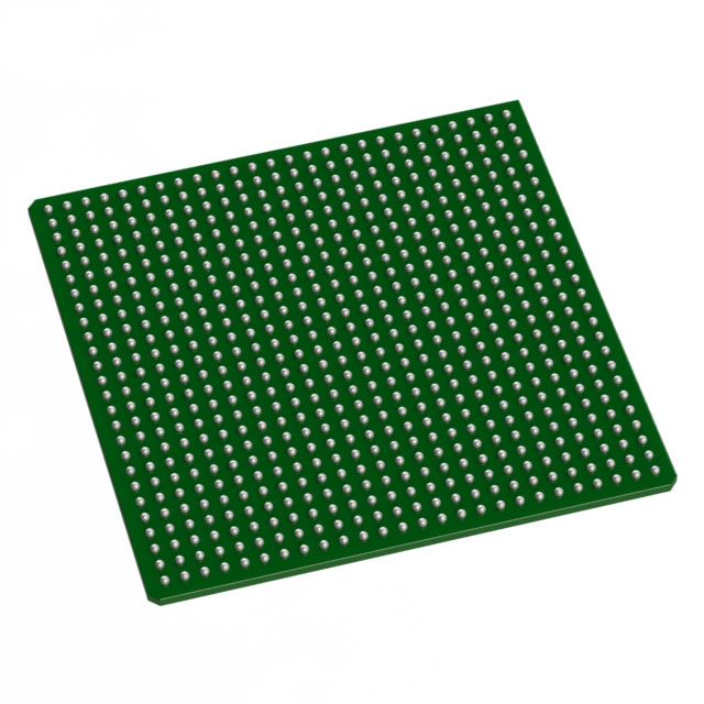
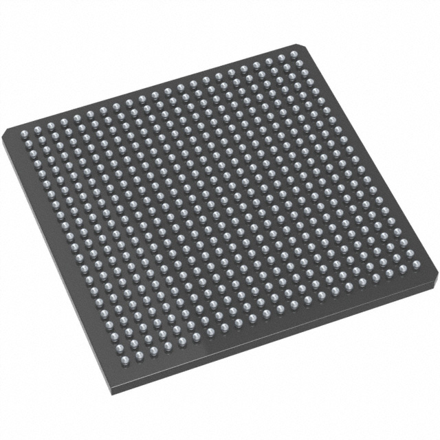
AX1000-2FGG484I
| Part Description |
Axcelerator Field Programmable Gate Array (FPGA) IC 317 165888 484-BGA |
|---|---|
| Quantity | 1,203 Available (as of June 15, 2026) |

| Product Category | Field Programmable Gate Array (FPGA) |
|---|---|
| Manufacturer | Microchip Technology |
| Manufacturing Status | Active |
| Manufacturer Standard Lead Time | 12 Weeks |
| Datasheet |
Specifications & Environmental
| Device Package | 484-FPBGA (23x23) | Grade | Industrial | Operating Temperature | -40°C – 85°C | ||
|---|---|---|---|---|---|---|---|
| Package / Case | 484-BGA | Number of I/O | 317 | Voltage | 1.425 V - 1.575 V | ||
| Mounting Method | Surface Mount | RoHS Compliance | ROHS3 Compliant | REACH Compliance | REACH Unaffected | ||
| Moisture Sensitivity Level | 3 (168 Hours) | Number of LABs/CLBs | 18144 | Number of Logic Elements/Cells | 18144 | ||
| Number of Gates | 1000000 | ECCN | 3A001A7A | HTS Code | 8542.39.0001 | ||
| Qualification | N/A | Total RAM Bits | 165888 |
Overview of AX1000-2FGG484I – Axcelerator Field Programmable Gate Array (FPGA) IC, 317 I/Os, 484-BGA
The AX1000-2FGG484I is an Axcelerator family FPGA using Microchip's AX antifuse architecture, delivering a single-chip, nonvolatile programmable solution with 1,000,000 equivalent system gates. It combines high-performance logic, embedded memory and flexible multi-standard I/Os in a compact 484-BGA package targeted at industrial applications requiring deterministic timing and robust in-system security.
Key Features
- Core Capacity and Logic — 1,000,000 equivalent system gates with 18,144 logic elements, providing substantial on-chip logic for complex designs.
- Embedded Memory and FIFOs — 165,888 bits of embedded SRAM/FIFO with programmable FIFO control logic to support buffering and high-throughput data paths.
- I/O Flexibility — 317 user I/Os with bank-selectable, mixed-voltage operation supporting 1.5V, 1.8V, 2.5V and 3.3V standards and differential interfaces such as LVDS and LVPECL.
- Performance — Architecture-level performance capabilities cited in the family datasheet, including 350+ MHz system performance and 500+ MHz internal performance for demanding timing requirements.
- Clocking and PLL — Segmentable clock resources and an embedded PLL with a 14–200 MHz input range and frequency synthesis capabilities up to 1 GHz (family-level feature).
- Power and Supply — Core supply specified at 1.425 V to 1.575 V (nominal 1.5 V) for low-power core operation.
- Package and Mounting — 484-BGA (484-FPBGA, 23 × 23) surface-mount package for compact board integration.
- Industrial Temperature Range — Rated for operation from −40 °C to 85 °C, suitable for industrial environments.
- Security and Test — Antifuse, nonvolatile programming technology (“FuseLock”) and JTAG boundary-scan support as described for the Axcelerator family.
- Compliance — RoHS compliant.
Typical Applications
- Industrial Control and Automation — Implement real-time control logic, sensor interfacing and deterministic timing in factory and process automation systems.
- High-Speed Data Interfaces — Support LVDS-capable I/Os and embedded FIFOs for data aggregation, protocol bridging and serial link buffering.
- Communications Infrastructure — Use embedded memory and high gate/count logic for packet processing, framing and custom protocol handling in networking equipment.
- Embedded System Integration — Consolidate glue logic, custom peripherals and timing-critical functions into a single, nonvolatile FPGA to reduce BOM and board area.
Unique Advantages
- Single-chip nonvolatile solution: Antifuse programming provides a one-time programmable, nonvolatile configuration that secures design IP and removes the need for external configuration memory.
- High logic density: 1,000,000 equivalent system gates and 18,144 logic elements enable complex, integrated designs without partitioning across multiple devices.
- Embedded RAM and FIFO support: 165,888 bits of on-chip memory with programmable FIFO control simplify data buffering and reduce external memory requirements.
- Flexible mixed-voltage I/Os: Bank-selectable multi-standard I/Os and differential signaling options allow interfacing with a wide range of peripherals and transceivers.
- Industrial temperature rating: −40 °C to 85 °C operation supports deployment in industrial environments with extended thermal requirements.
- Compact BGA footprint: 484-FPBGA (23 × 23) package provides a space-efficient option for high-pin-count FPGA integration.
Why Choose AX1000-2FGG484I?
The AX1000-2FGG484I delivers a balanced combination of high logic capacity, embedded memory, and flexible I/O in a single nonvolatile FPGA targeted at industrial designs. Its antifuse-based AX architecture offers deterministic timing, on-chip FIFOs and multi-standard I/O support—features that simplify system architecture and reduce external component count.
This device is well suited to engineers and procurement teams building high-performance embedded systems, telecommunications modules, and industrial control equipment that require secure, one-time-programmable logic, compact packaging and industrial temperature operation. The Axcelerator family-level capabilities provide a clear upgrade path for designs needing greater density or additional interfaces.
Request a quote or submit a procurement inquiry today to check availability and obtain pricing information for the AX1000-2FGG484I.


Date Founded: 1989
Headquarters: Chandler, Arizona, USA
Employees: 22,000+
Revenue: $8.349 Billion
Certifications and Memberships: ISO9001:2015, IATF16949:2016, AS 9100D


