
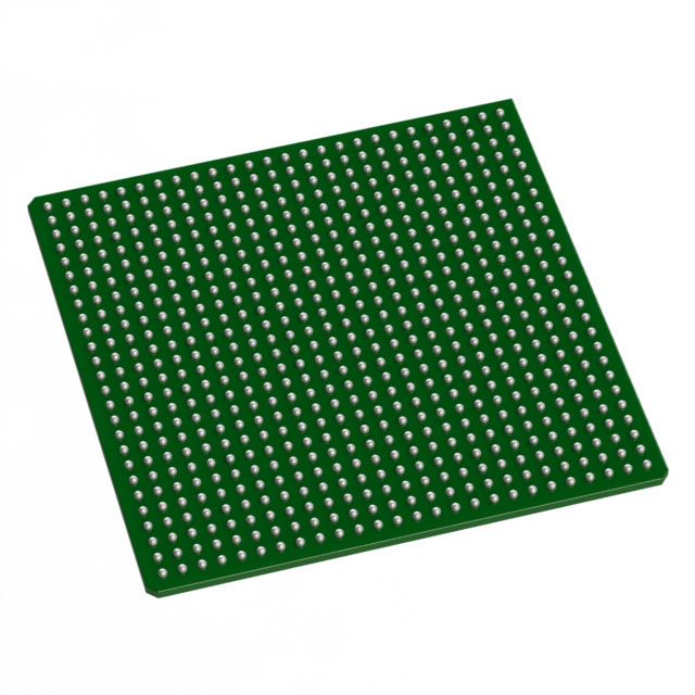
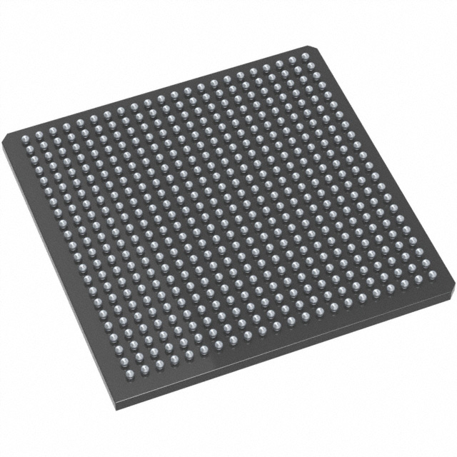
AX1000-2FGG676I
| Part Description |
Axcelerator Field Programmable Gate Array (FPGA) IC 418 165888 676-BGA |
|---|---|
| Quantity | 218 Available (as of June 10, 2026) |

| Product Category | Field Programmable Gate Array (FPGA) |
|---|---|
| Manufacturer | Microchip Technology |
| Manufacturing Status | Active |
| Manufacturer Standard Lead Time | 12 Weeks |
| Datasheet |
Specifications & Environmental
| Device Package | 676-FBGA (27x27) | Grade | Industrial | Operating Temperature | -40°C – 85°C | ||
|---|---|---|---|---|---|---|---|
| Package / Case | 676-BGA | Number of I/O | 418 | Voltage | 1.425 V - 1.575 V | ||
| Mounting Method | Surface Mount | RoHS Compliance | ROHS3 Compliant | REACH Compliance | REACH Unaffected | ||
| Moisture Sensitivity Level | 3 (168 Hours) | Number of LABs/CLBs | 18144 | Number of Logic Elements/Cells | 18144 | ||
| Number of Gates | 1000000 | ECCN | 3A001A7A | HTS Code | 8542.39.0001 | ||
| Qualification | N/A | Total RAM Bits | 165888 |
Overview of AX1000-2FGG676I – Axcelerator Field Programmable Gate Array (FPGA) IC 418 165888 676-BGA
The AX1000-2FGG676I is an Axcelerator antifuse FPGA from Microchip Technology built on the AX architecture. It is a single-chip, nonvolatile FPGA offering deterministic timing and system-level features including segmentable clocks, PLLs and embedded SRAM with FIFO control logic.
Designed for industrial applications, this device delivers high internal performance and flexible I/O capabilities while providing hardware-level programming protection. Key device parameters include 1,000,000 equivalent system gates, 18,144 logic elements, 418 user I/Os and approximately 0.166 Mbits of embedded memory.
Key Features
- Core Architecture
Antifuse-based AX architecture provides a single-chip, nonvolatile solution with deterministic and user-controllable timing. - Logic Capacity
Approximately 1,000,000 equivalent system gates implemented as 18,144 logic elements to support complex logic and control functions. - Embedded Memory & FIFOs
Approximately 0.166 Mbits (165,888 bits) of on-chip SRAM with embedded FIFO control logic and independently width-configurable read/write ports. - High-Performance Timing
Segmentable clock resources plus an embedded PLL (14–200 MHz input range, frequency synthesis up to 1 GHz) support high-speed internal operation and flexible clocking. - I/O Flexibility
418 user I/Os with support for mixed-voltage operation and differential standards; datasheet notes LVDS-capable I/Os and high-speed signaling options. - Performance
Datasheet-cited performance: 350+ MHz system performance and 500+ MHz internal performance to address demanding processing paths. - Security & Reliability
FuseLock™ programming technology provides protection against reverse engineering and design theft; device is a single-chip nonvolatile solution. - Package & Industrial Grade
676-ball FBGA (27 × 27 mm) surface-mount package; industrial temperature grade with an operating range of −40 °C to +85 °C and core supply 1.425 V to 1.575 V. RoHS compliant.
Typical Applications
- Industrial Control
Deterministic timing, industrial temperature rating and high logic density make the device suitable for complex control and sequencing tasks. - High-Speed Data Interfaces
High internal performance, embedded FIFOs and LVDS-capable I/Os support protocol bridging and high-throughput data paths. - Telecommunications and Networking
Segmentable clocks, embedded PLL and flexible I/O standards enable timing-sensitive packet processing and interface adaptation. - Instrumentation & Test Equipment
Large logic capacity and on-chip RAM/FIFO resources are useful for fast signal acquisition, buffering and real-time processing.
Unique Advantages
- Nonvolatile, one-time programmable architecture
Antifuse-based single-chip solution eliminates the need for external configuration memory and provides stable, permanent configuration. - High integration reduces system BOM
On-chip SRAM, embedded FIFO control logic and PLLs minimize external components for buffering, clocking and memory. - Security-conscious programming
FuseLock™ programming technology protects intellectual property by preventing reverse engineering and design theft. - Deterministic timing and debug
User-controllable timing, segmentable clocking and in-system diagnostic capability support precise timing design and validation workflows. - Industrial-ready mechanical and electrical specs
Surface-mount 676-FBGA package, industrial temperature range and RoHS compliance simplify integration into production systems.
Why Choose AX1000-2FGG676I?
The AX1000-2FGG676I is positioned for designs that require permanent, high-density logic with deterministic performance and built-in security. With 18,144 logic elements, embedded SRAM/FIFO resources and a high I/O count, it addresses complex interface, buffering and processing requirements while eliminating external configuration memory.
This device is well suited to industrial and communications equipment where timing control, in-system diagnostics and IP protection are important. Its combination of processing performance, integrated memory and flexible I/O makes it a practical choice for engineers seeking a robust, long-term FPGA solution backed by Microchip's Axcelerator architecture.
Request a quote or submit a pricing and availability inquiry to receive product-level information and support for your design evaluation and procurement process.


Date Founded: 1989
Headquarters: Chandler, Arizona, USA
Employees: 22,000+
Revenue: $8.349 Billion
Certifications and Memberships: ISO9001:2015, IATF16949:2016, AS 9100D


