
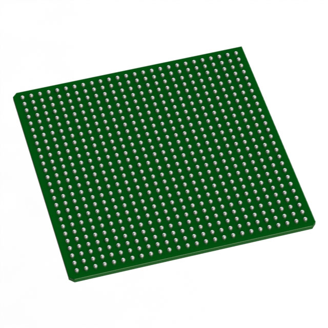
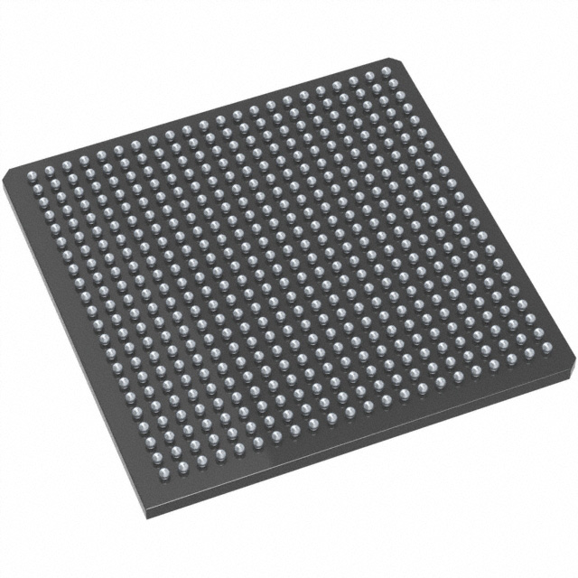
AX1000-BG729
| Part Description |
Axcelerator Field Programmable Gate Array (FPGA) IC 516 165888 729-BBGA |
|---|---|
| Quantity | 124 Available (as of June 10, 2026) |

| Product Category | Field Programmable Gate Array (FPGA) |
|---|---|
| Manufacturer | Microchip Technology |
| Manufacturing Status | Active |
| Manufacturer Standard Lead Time | 52 Weeks |
| Datasheet |
Specifications & Environmental
| Device Package | 729-PBGA (35x35) | Grade | Commercial | Operating Temperature | 0°C – 70°C | ||
|---|---|---|---|---|---|---|---|
| Package / Case | 729-BBGA | Number of I/O | 516 | Voltage | 1.425 V - 1.575 V | ||
| Mounting Method | Surface Mount | RoHS Compliance | RoHS non-compliant | REACH Compliance | REACH Unaffected | ||
| Moisture Sensitivity Level | 3 (168 Hours) | Number of LABs/CLBs | 18144 | Number of Logic Elements/Cells | 18144 | ||
| Number of Gates | 1000000 | ECCN | 3A001A7A | HTS Code | 8542.39.0001 | ||
| Qualification | N/A | Total RAM Bits | 165888 |
Overview of AX1000-BG729 – Axcelerator FPGA, 516 I/Os, ~0.166 Mbits Embedded RAM, 729‑BBGA
The AX1000-BG729 is an Axcelerator family Field Programmable Gate Array (FPGA) device built on Microchip’s AX architecture and antifuse-based, nonvolatile programming technology. The device delivers a combination of high system and internal performance, flexible multi‑standard I/Os, and on‑chip embedded SRAM/FIFO resources suitable for designs requiring deterministic timing, secure programming, and high I/O density.
AX1000 combines system-level capabilities—segmentable clocks, embedded PLLs, chip‑wide routing and embedded FIFO control logic—with a high logic capacity and a 729‑ball BGA package, providing an integrated platform for complex digital designs within commercial temperature ranges.
Key Features
- Core Capacity Provides 1,000,000 equivalent system gates and 18,144 logic elements (cells) to implement substantial custom logic on a single nonvolatile device.
- Embedded Memory & FIFOs Includes 36 core RAM blocks delivering approximately 0.166 Mbits of embedded memory with programmable FIFO control logic and variable-aspect 4,608‑bit RAM block organization options.
- High‑Performance Timing Documented system performance of 350+ MHz and internal performance of 500+ MHz, with segmentable clock resources and deterministic, user‑controllable timing.
- Advanced PLLs Embedded PLLs support a 14–200 MHz input range and frequency synthesis capabilities up to 1 GHz for flexible clock generation and management.
- Flexible, High‑Speed I/Os Up to 516 user I/Os supporting mixed voltages (1.5V, 1.8V, 2.5V, 3.3V), a wide range of single‑ended and differential standards, and LVDS channels capable of 700 Mb/s.
- Secure, Nonvolatile Programming Antifuse programming with FuseLock technology provides a single‑chip, nonvolatile solution that protects designs against reverse engineering and unauthorized duplication.
- Package & Supply Surface‑mount 729‑BBGA package (supplier package: 729‑PBGA, 35×35 mm); core voltage supply range is 1.425 V to 1.575 V.
- Commercial Grade & Compliance Rated for 0 °C to 70 °C operating temperature and RoHS compliant.
Typical Applications
- High‑speed serial I/O systems Leverage LVDS‑capable I/Os and high internal performance for board‑level high‑throughput interfaces and data links.
- Memory‑intensive buffering and FIFO management Built‑in RAM blocks and programmable FIFO control logic provide on‑chip buffering for streaming data and protocol bridging.
- Deterministic clocked logic Segmentable clocks and integrated PLLs enable precise timing control for synchronous digital subsystems.
- Secure, nonvolatile logic deployment Antifuse programming and FuseLock technology secure intellectual property in deployed systems that require permanent configuration.
Unique Advantages
- High logic density: 1,000,000 equivalent gates and 18,144 logic elements let you consolidate complex functions into a single device and reduce board-level BOM.
- On‑chip memory and FIFO control: 36 RAM blocks (≈0.166 Mbits) with configurable widths and embedded FIFO logic simplify data buffering and reduce external memory requirements.
- Deterministic performance: Segmentable clocks, deterministic timing and integrated PLLs provide predictable timing for real‑time and latency‑sensitive designs.
- Broad I/O flexibility: Bank‑selectable, mixed‑voltage I/Os and support for multiple single‑ended and differential standards enable straightforward interfacing to diverse peripherals and subsystems.
- Secure, one‑time programmable design: Antifuse programming with FuseLock protects IP and prevents reverse engineering, supporting secure product deployment.
- Commercial temperature and RoHS compliance: Suited for commercial applications requiring RoHS‑compliant components within 0 °C to 70 °C.
Why Choose AX1000-BG729?
AX1000-BG729 positions itself as a high‑capacity, nonvolatile FPGA optimized for designs that need a combination of high logic density, embedded memory/FIFO capability, and flexible, high‑speed I/O in a compact BGA package. Its AX architecture elements—segmentable clocks, PLLs, and chip‑wide routing—support deterministic performance and complex system integration.
This device is well suited for engineering teams that require a secure, on‑chip programmable solution with significant on‑die RAM and I/O resources, enabling reduced component count, simplified board design, and long‑term deployment stability within commercial temperature ranges.
Request a quote or submit a request for pricing and availability for the AX1000-BG729 to evaluate how this Axcelerator FPGA fits your next design.


Date Founded: 1989
Headquarters: Chandler, Arizona, USA
Employees: 22,000+
Revenue: $8.349 Billion
Certifications and Memberships: ISO9001:2015, IATF16949:2016, AS 9100D


